Open-sourcing a 205W buck-boost fast-charging module (140W+65W) based on the IP6557 and IP6538 chips. One Type-C port supports the PD3.1 protocol, with a maximum output of 28V5A. The other ports include a Type-C and a Type-A, with a combined maximum output of 65W (20V3.25A). Pair it with a 24V10A switching power supply, and you can assemble a cost-effective 205W fast charger! Maximum conversion efficiency reaches 96.7%.
If you have suggestions for improvement, feel free to leave a friendly comment below.
Full documentation is provided, allowing you to replicate the design yourself. The download link is at the end of this post!
Video demo: https://www.youtube.com/watch?v=H3SJjzX0Zzg
Open-source project link on the LCSC Open Source Platform: https://url.zeruns.tech/99439
Electronics/MCU technical discussion QQ group: 820537762
Introduction
Pair this fast-charging module with a 24V10A switching power supply to create a cost-effective dual-channel 205W fast charger! (Second-hand power supplies with a voltage of 24 volts and a current of 10 amperes can probably be bought at around 30 yuan.)
With an adapter cable that converts a cigarette lighter socket to a DC male/XT30 interface, it can also be turned into a car charger—a 140W+65W in-car fast charger!
The module has two input interfaces: XT30 and DC5.5 (These two input interfaces cannot be used simultaneously, as they are connected in parallel!).
Input voltage range for the module: 8.2~31V.
The C1 port supports buck-boost conversion, allowing the input voltage to be lower than the output. The C2 and A ports are buck-only, meaning the output voltage must be lower than the input voltage.
I purchased 8 IP6557 chips and soldered them all. Four of them were defective (with various issues), while the other four worked fine. I'm unsure whether this is due to chip quality/control issues or my soldering process (I set the hot plate temperature to 230°C with no signs of faulty-welding). On the other hand, all the IP6538 chips worked flawlessly without any issues. Both chips were purchased from the same store.
I’ve made a few finished units. If you’re interested in buying one, join the group and ask.
Parameters and Overview
C1 Port (IP6557)
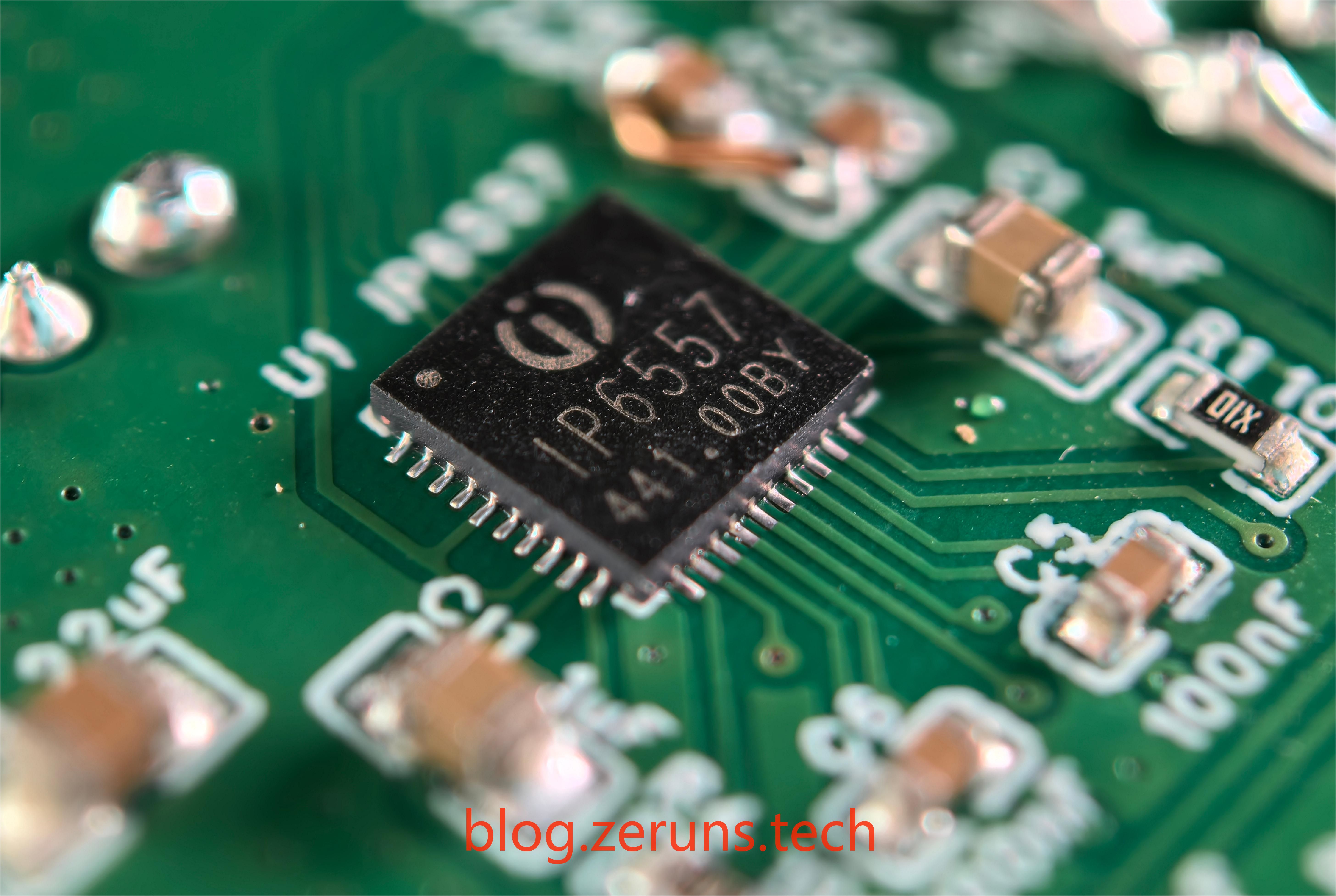
The first Type-C power chip is the IP6557-C from INJOINIC, with a maximum output power of 140W, supporting up to 28V/5A (can reach up to 6A in practice).
Input Voltage Range: 5–31V
This chip features buck-boost conversion, allowing the output voltage to exceed the input voltage.
Supported fast charging protocols include:
- PD3.1 / PPS / ERP28V
- BC1.2 and Apple
- QC2.0 / QC3.0 / QC3+ / QC4+ / QC5
- FCP and HSCP
- AFC
- MTK
- UFCS (Universal Fast Charging Specification)
Supports output voltages of 5V, 9V, 12V, 15V, 20V, and 28V.
PPS supports voltage outputs from 3.3V to 21V, adjustable in 10mV steps.
C2 and A1 Ports (IP6538)
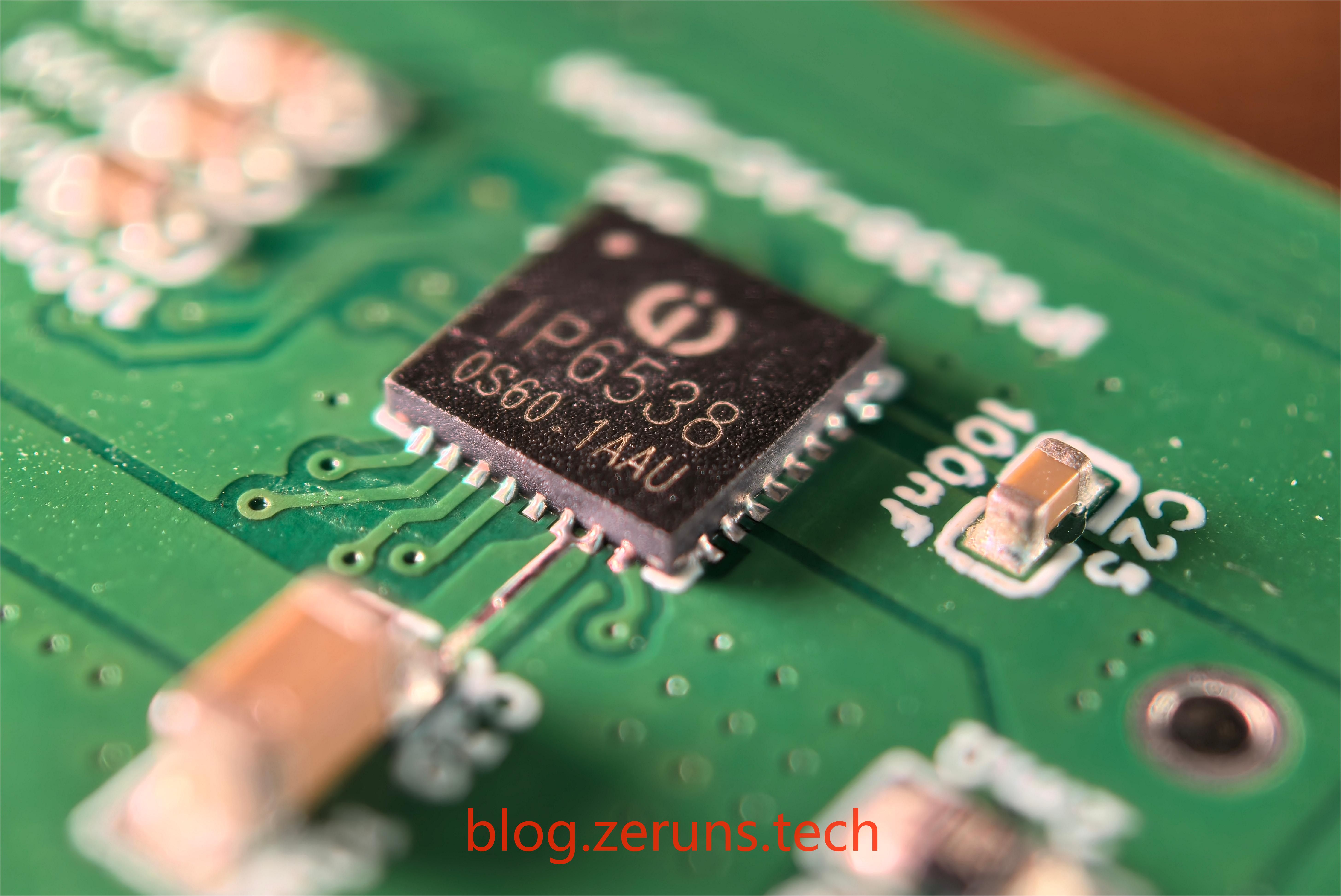
The second Type-C port and the Type-A port use the IP6538-AC-65W chip. When a single Type-C port is used, it supports up to 20V/3.25A, with a maximum power of 65W. When both ports are used simultaneously, they both output 5V, with a total power of 5V/4.8A.
Input Voltage Range: 8.2–32V (shared input port with the first chip, so the actual maximum is 31V).
This chip is a buck-only converter, meaning the output voltage cannot exceed the input voltage. To achieve the full 65W output, the input voltage must be at least 21V.
Note: The IP6538 chip comes in two versions: 45W and 65W. Chips without the "-65W" suffix are the 45W version! (The documentation provided below includes the datasheet for the 45W version; a datasheet for the 65W version is unavailable.)
Supported fast charging protocols include:
- PD2.0 / PD3.0 (PPS); the Type-A port does not support PD protocols.
- BC1.2, Apple, and Samsung protocols.
- QC2.0 and QC3.0.
- MTK PE+1.1 and MTK PE+2.0.
- Huawei fast charge protocols: FCP / SCP.
- Samsung fast charge protocol: AFC.
- Spreadtrum fast charge protocol: SFCP.
- OPPO fast charge protocols: VOOC / Super VOOC (The 65W version of the chip appears not to support OPPO fast charge protocols. The 45W version hasn’t been tested—original cables may be required to activate these protocols.)
Supports output voltages of 5V, 9V, 12V, 15V, and 20V.
PPS supports voltage outputs from 3.3V to 11V, adjustable in 20mV steps.
Real Object Photos
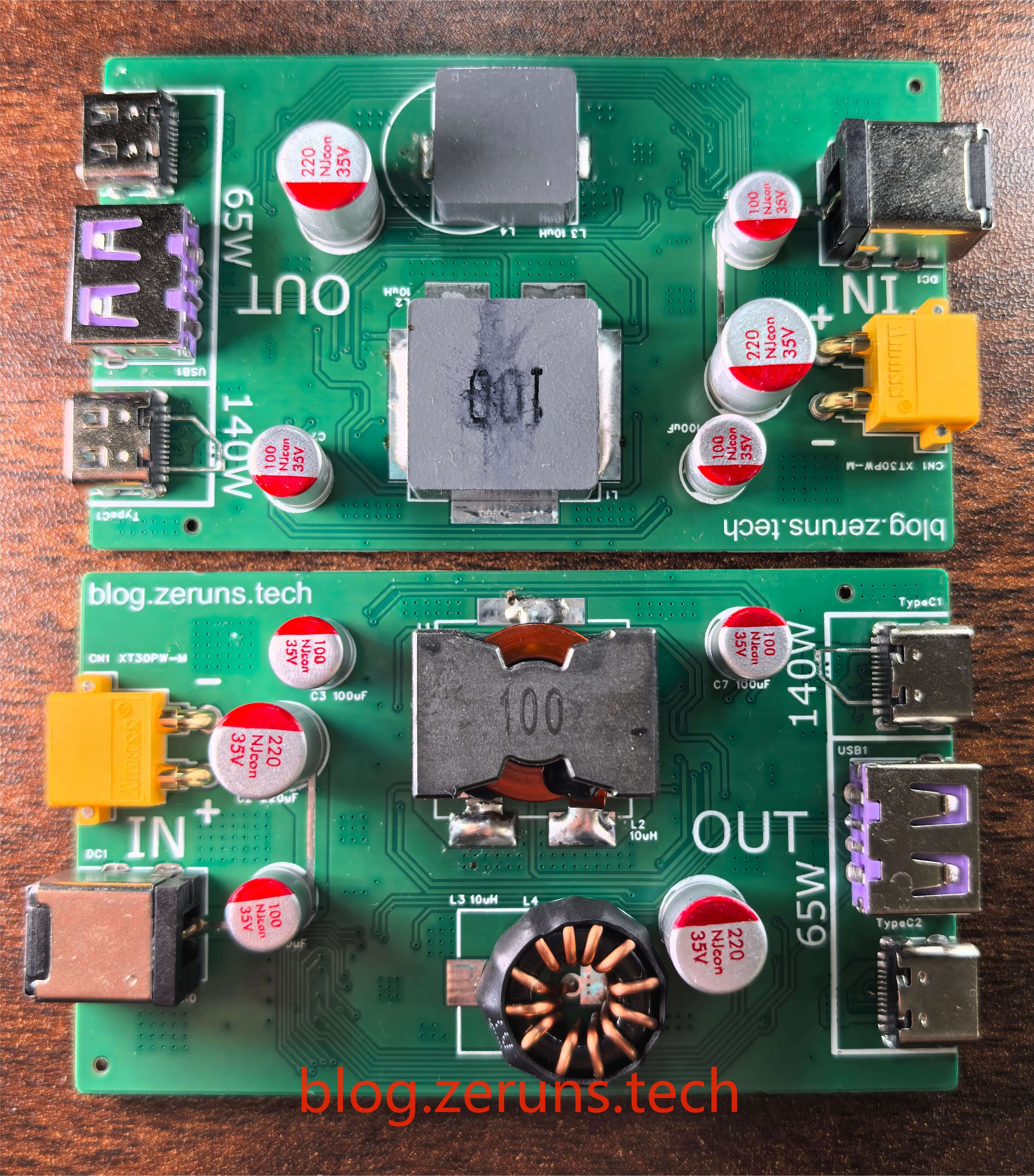
Front of the PCB
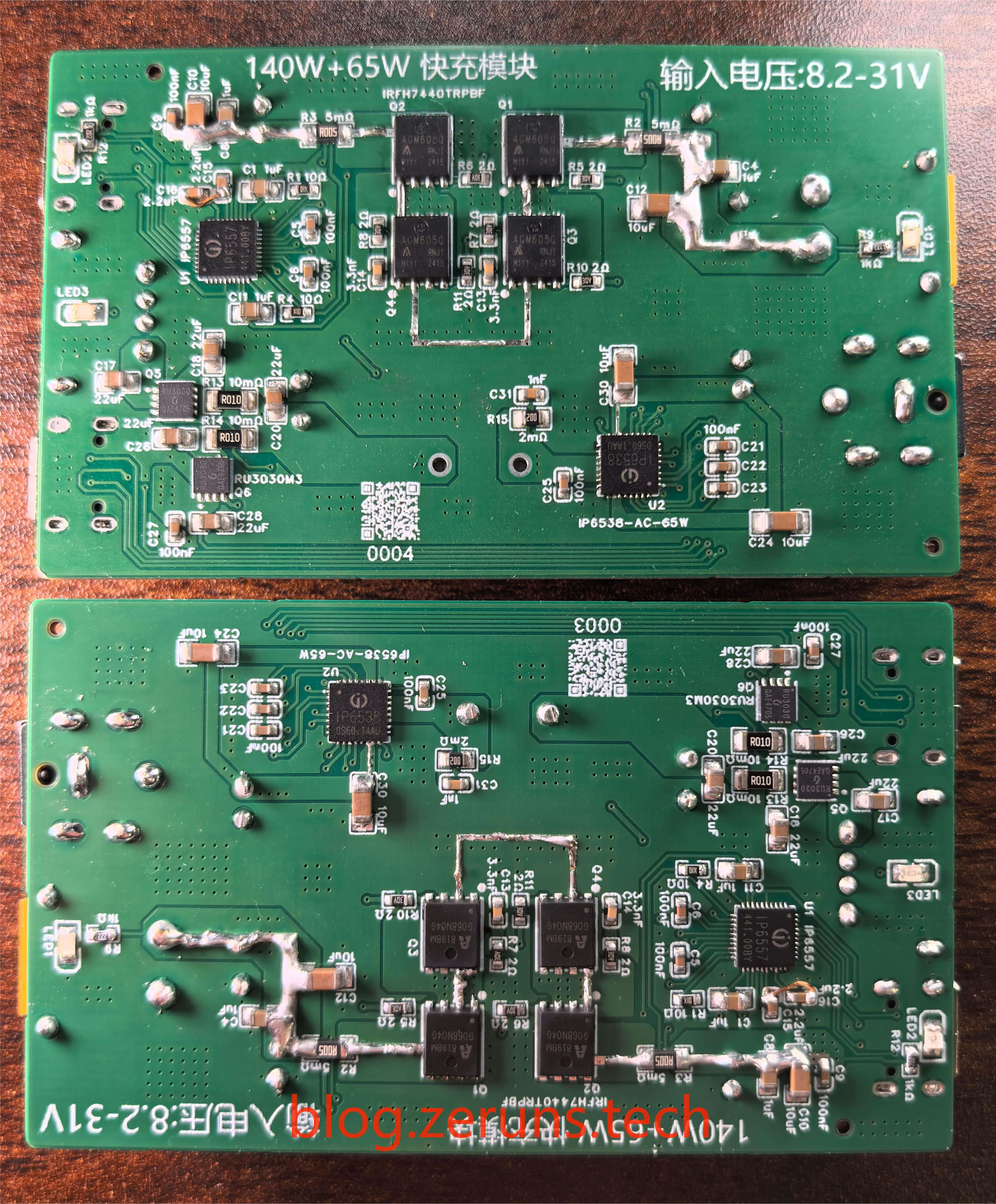
Back of the PCB
The jumper wires shown in the image below are due to an error caused by the application schematic in the INJOINIC official datasheet. The crossing lines in the schematic were not marked as connected, leading to a mistake in my design. This was corrected with the jumper wires. The published schematic and PCB files have been fixed.
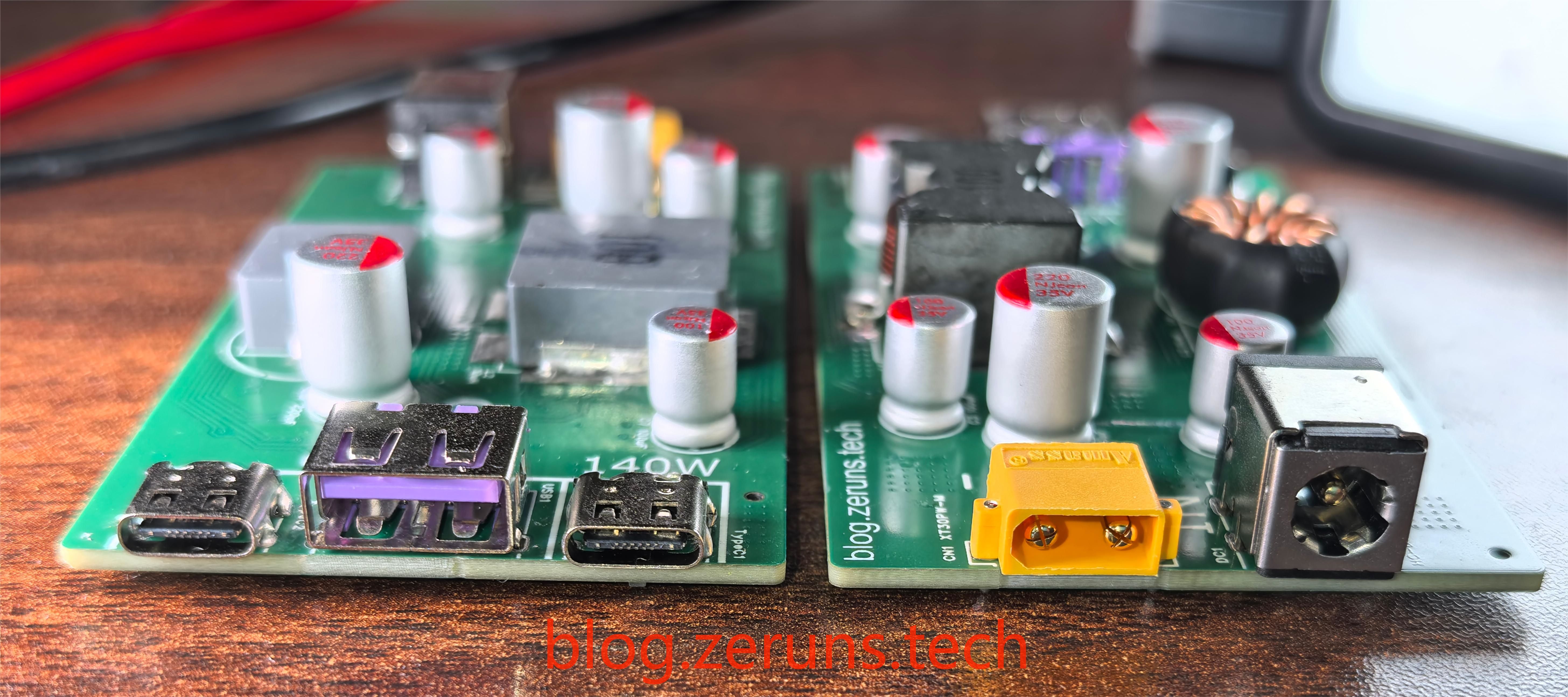
Side View of the PCB
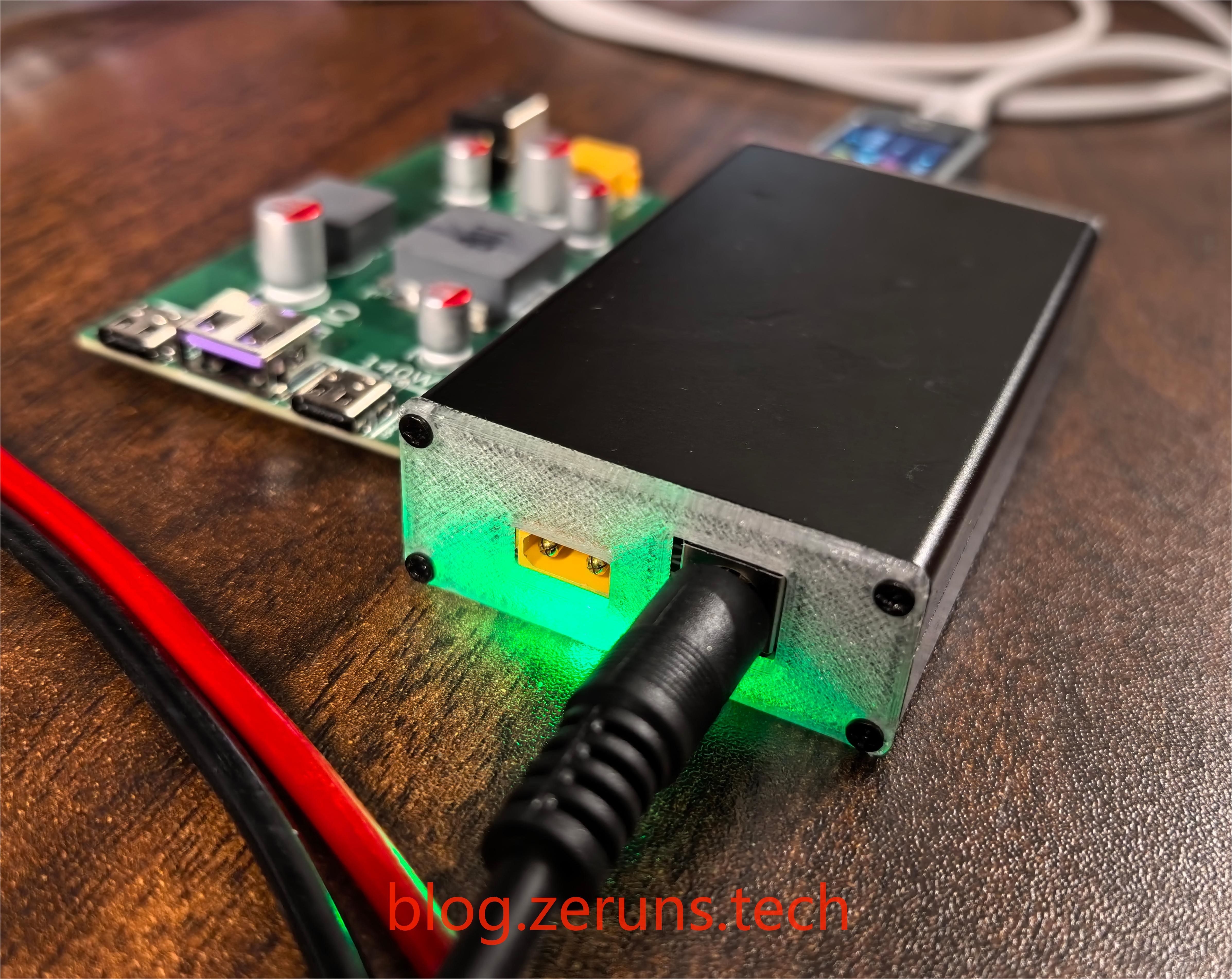
With the Enclosure Installed
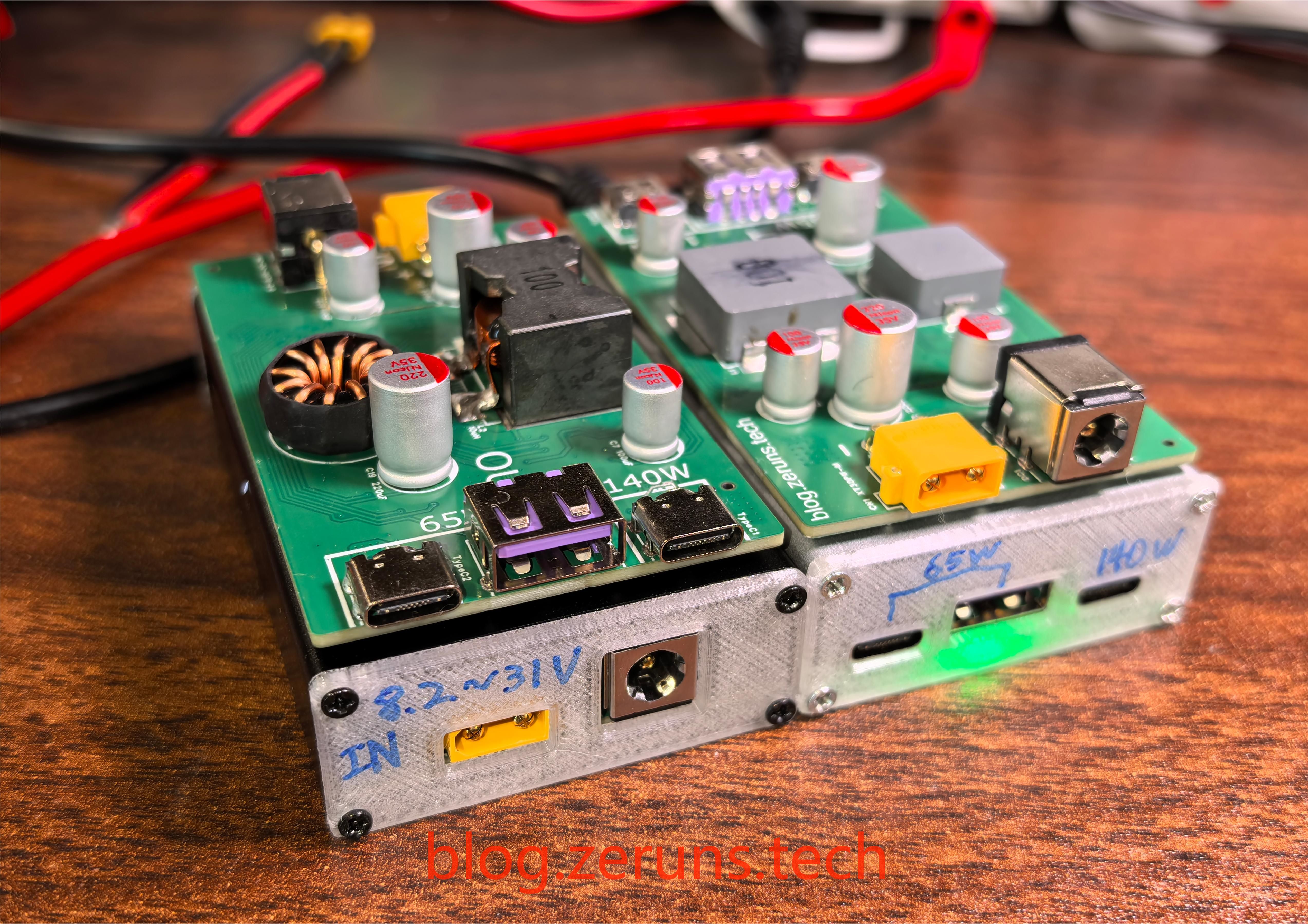
The aluminum enclosure was purchased as a finished product, and the front and back covers were custom 3D-printed.
Unboxing experience of the Bambu Lab P1SC 3D printer: https://blog.zeruns.tech/archives/770.html
Close-up of the Soldered IP6557 Chip
Close-up of the Soldered IP6538 Chip
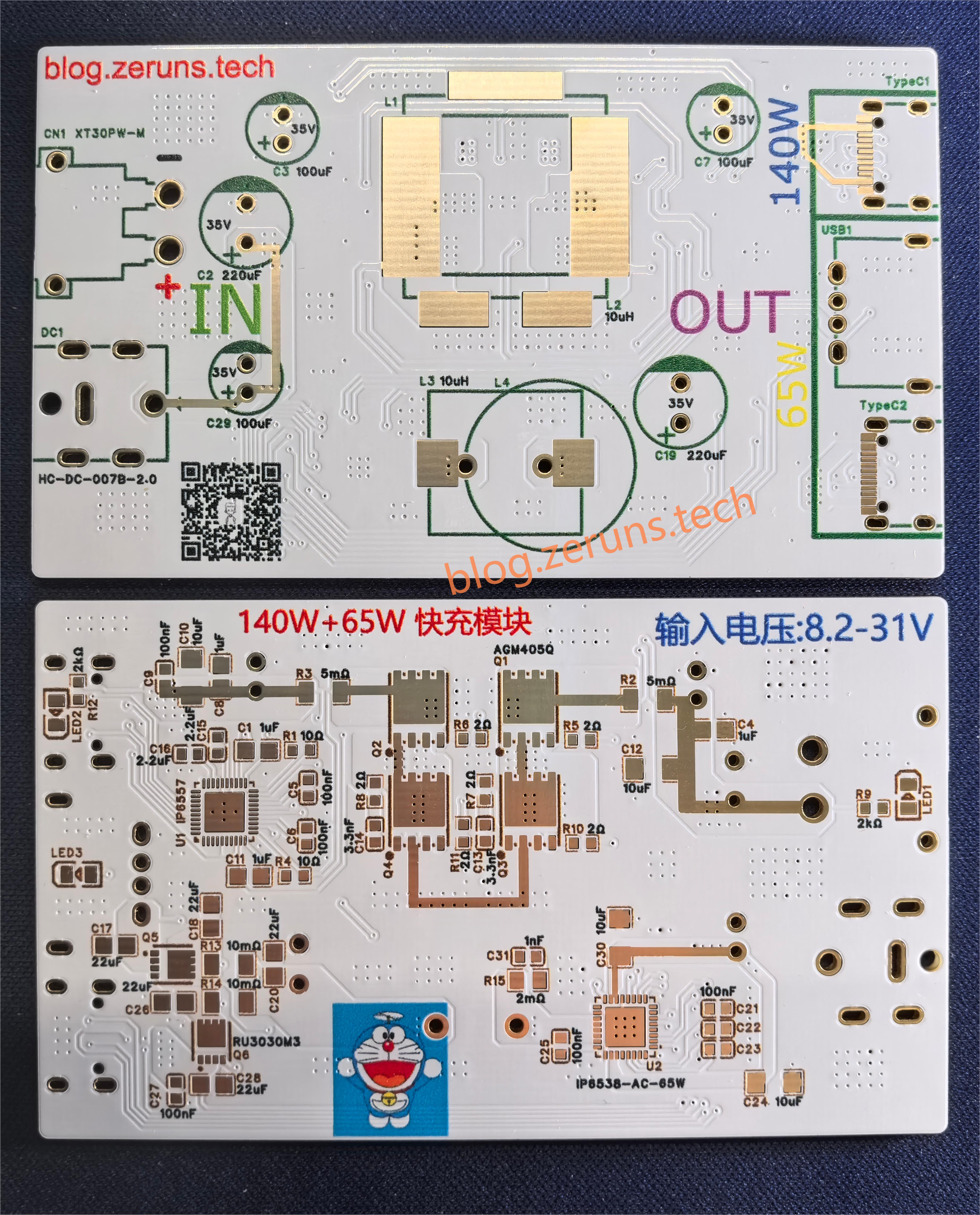
Experimenting with Color Silkscreen
Instructions & Notes
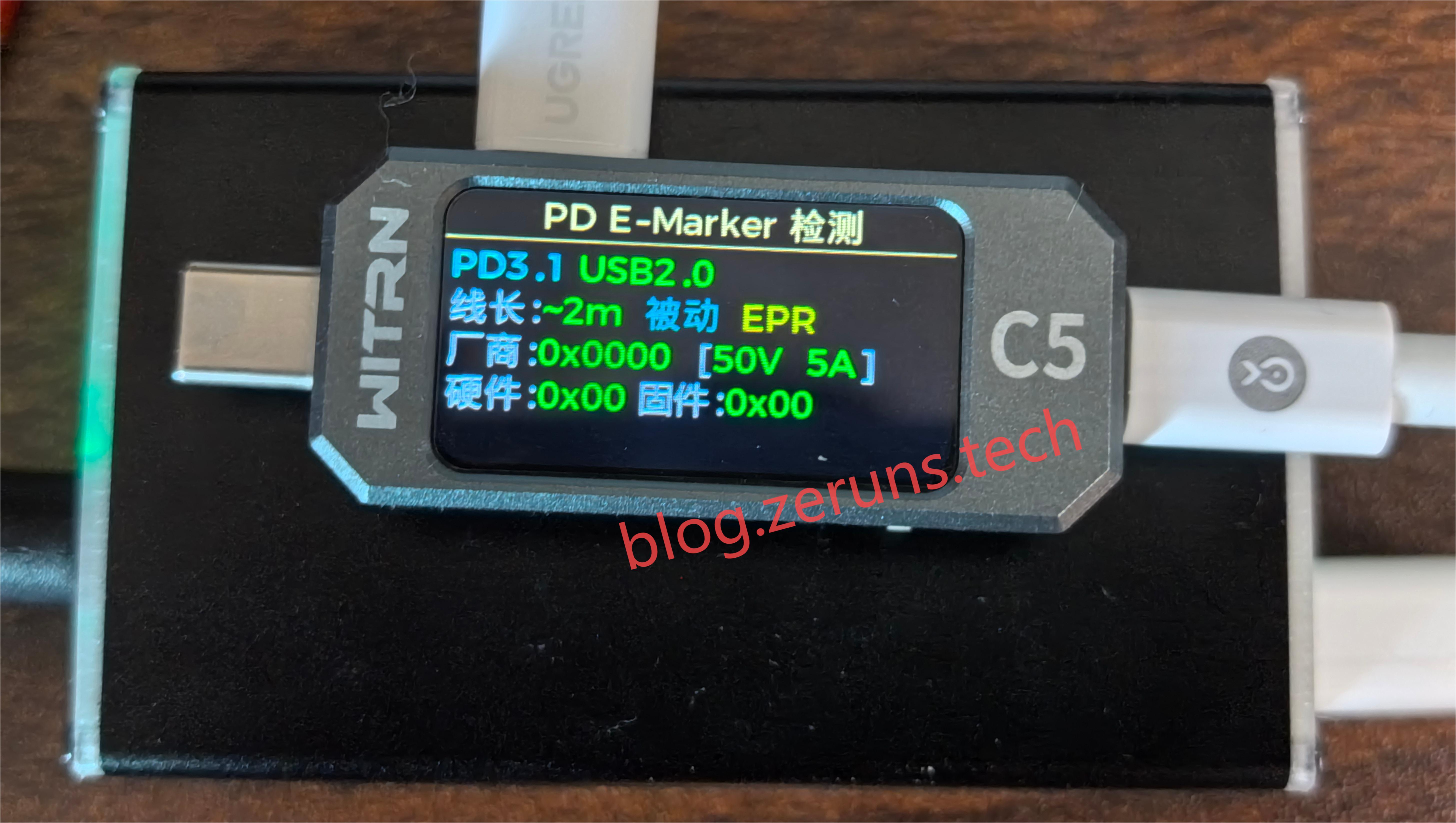
1. To achieve an output of 28V/5A, you must use a data cable with an E-Marker chip that supports the PD3.1 protocol, as shown below.
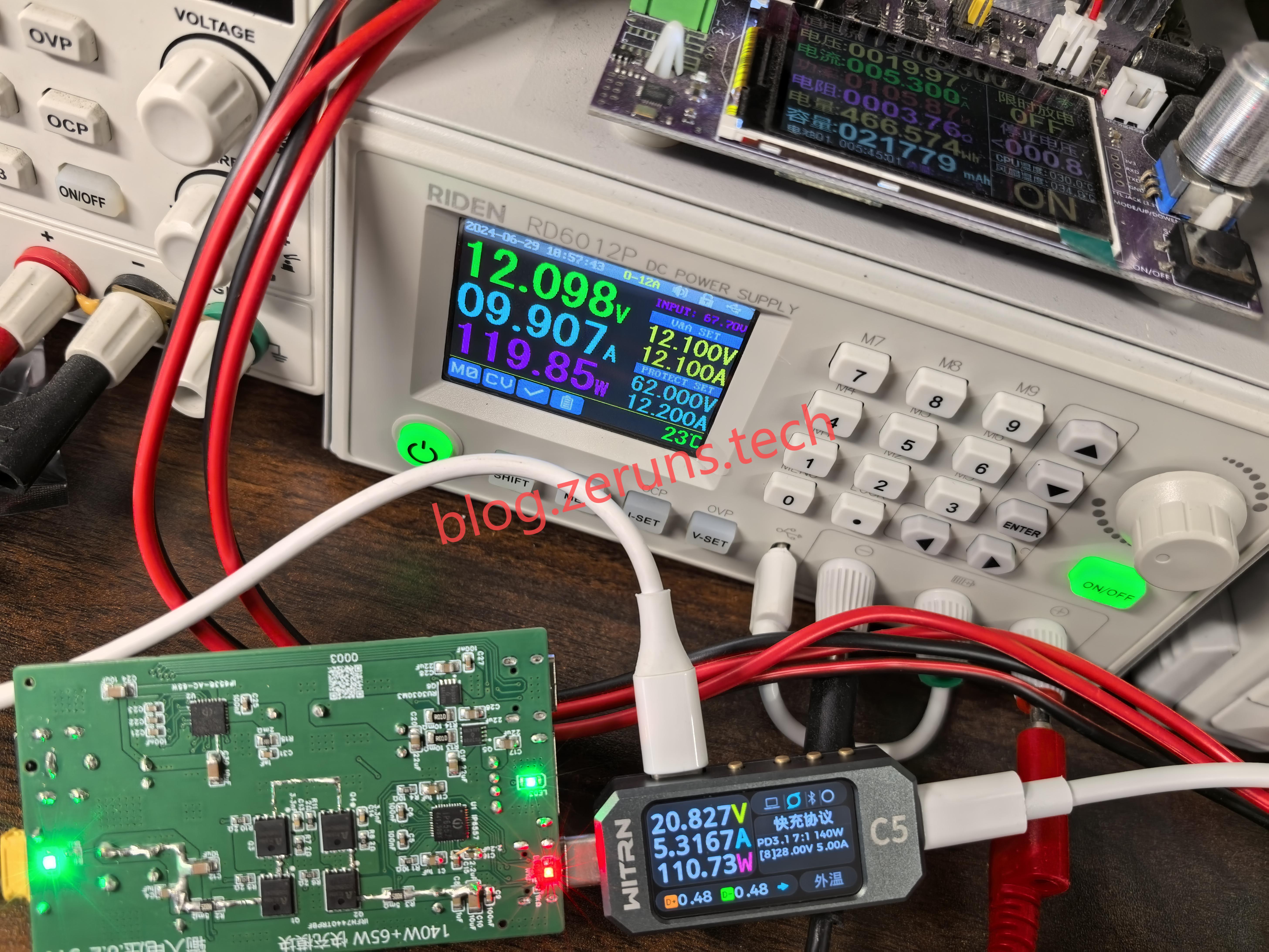
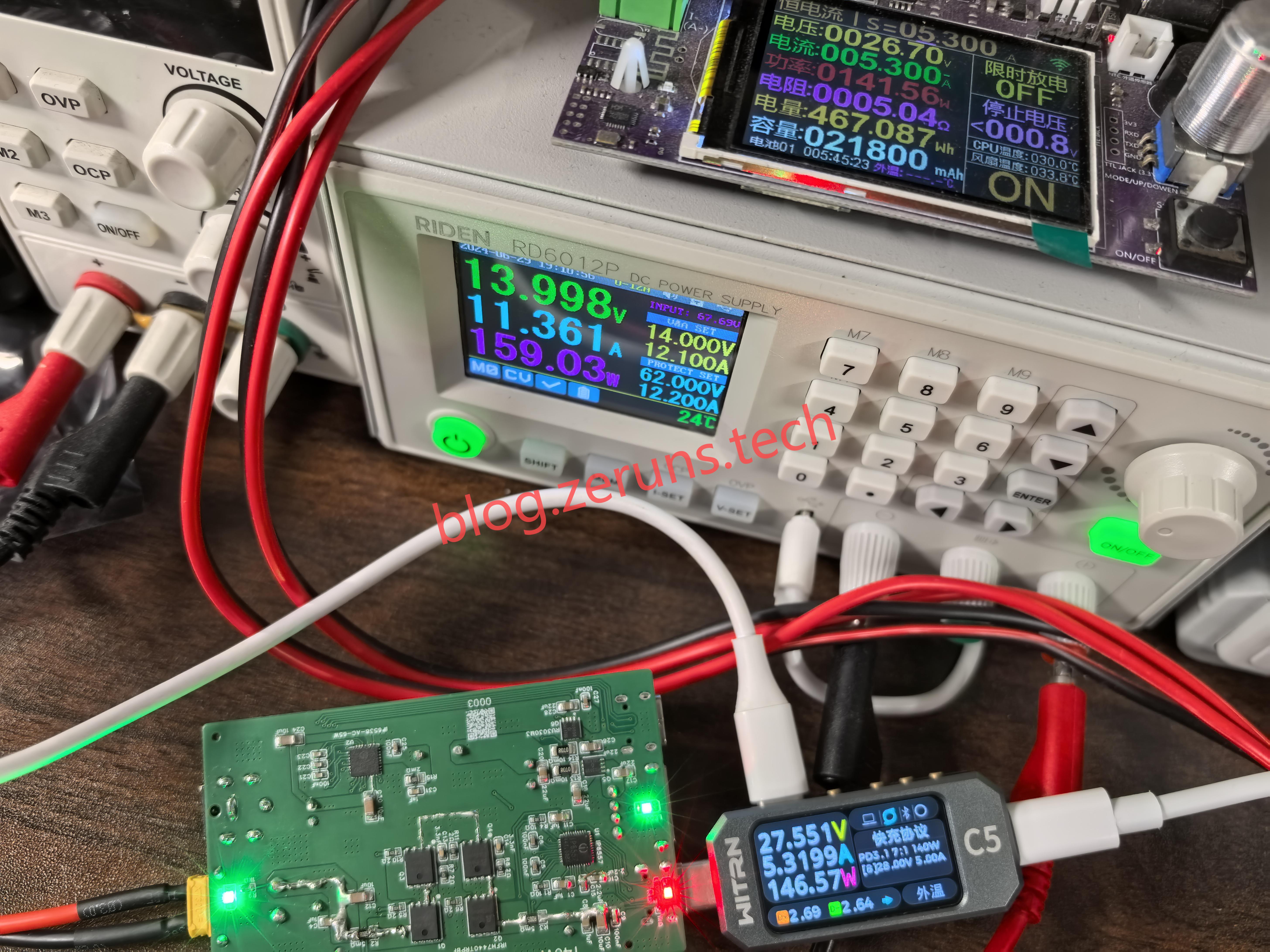
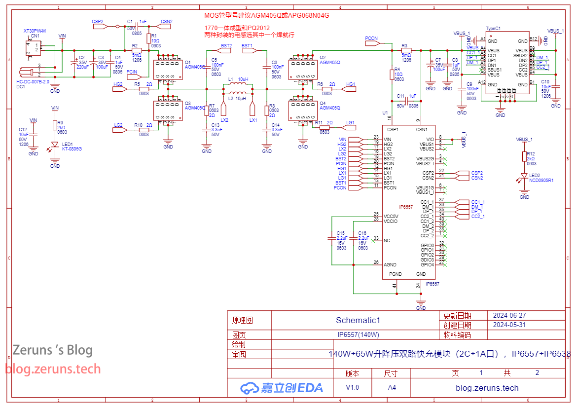
2. The board's input current sampling resistor (shunt resistor) R2 has a value of 5mΩ, with the IP6557 chip's input current limit set at 10A. If the input voltage is 12V, the current required to output 140W is at least 12A. Exceeding the limit will cause the output voltage to drop, making it impossible to reach full power. You can replace R2 with a resistor of a lower value, such as 2.5mΩ (e.g., two 5mΩ resistors in parallel). This allows full power output even at a 12V input. However, with the higher current, the MOSFETs will generate significant heat, so proper cooling is essential!
The two images below compare performance before and after modifying the shunt resistor. In the first image, the input current is limited to under 10A; in the second image, after the modification, the input current exceeds 10A, enabling a 28V/5A output at a 12V input. Since my adjustable power supply is limited to 12A, I set the input voltage to 14V for the test.
3. If you opt to use alternative MOSFETs, ensure that the MOSFET's Ciss parameter is less than 1000pF. Since the IP6557 operates at a switching frequency of 250kHz, higher switching frequencies impose stricter requirements on the MOSFET's input capacitance. Excessive Ciss will affect the MOSFET's switching times.
Protocol Support Testing
The protocols supported by the C1 port are shown below:
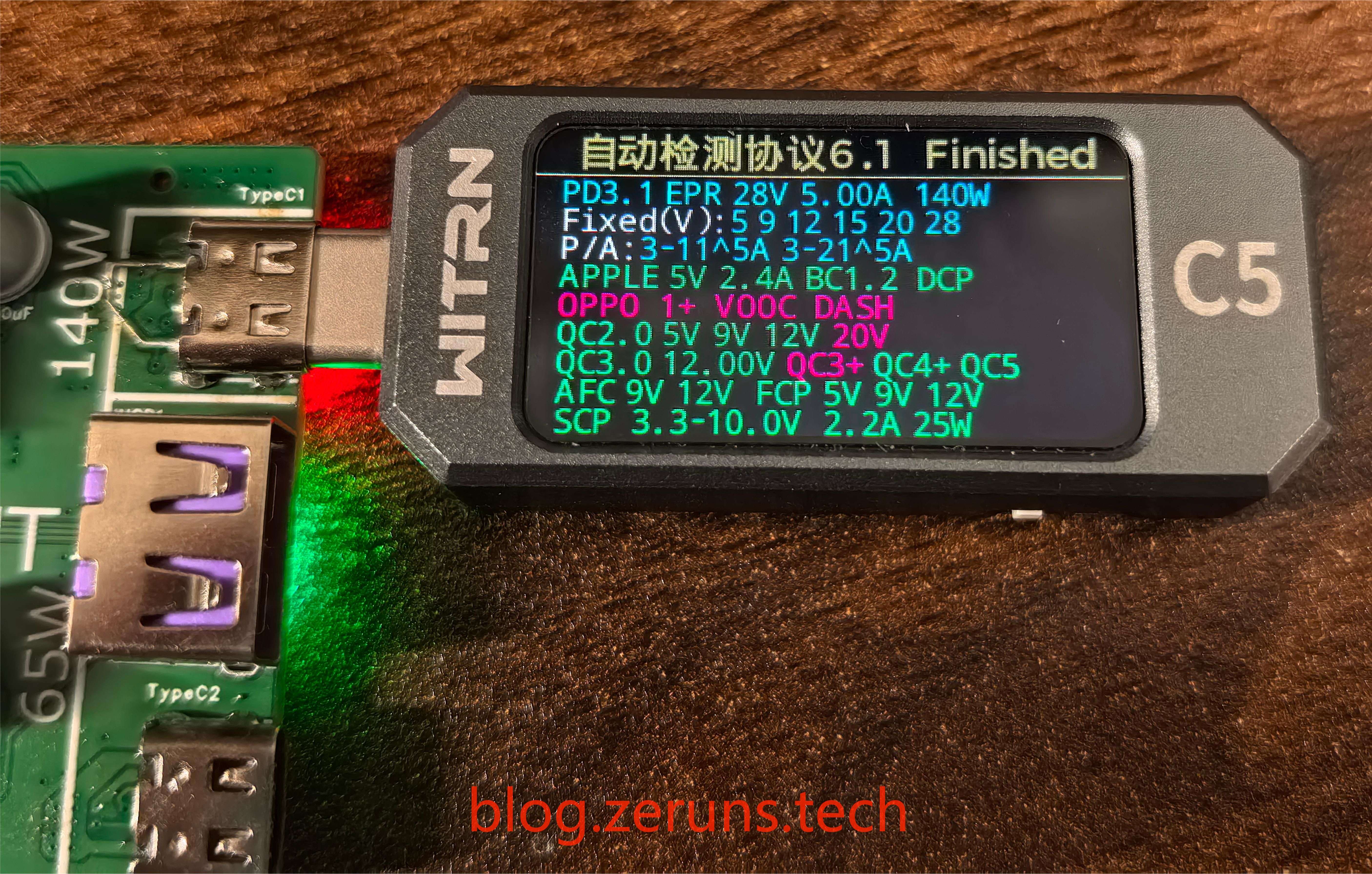
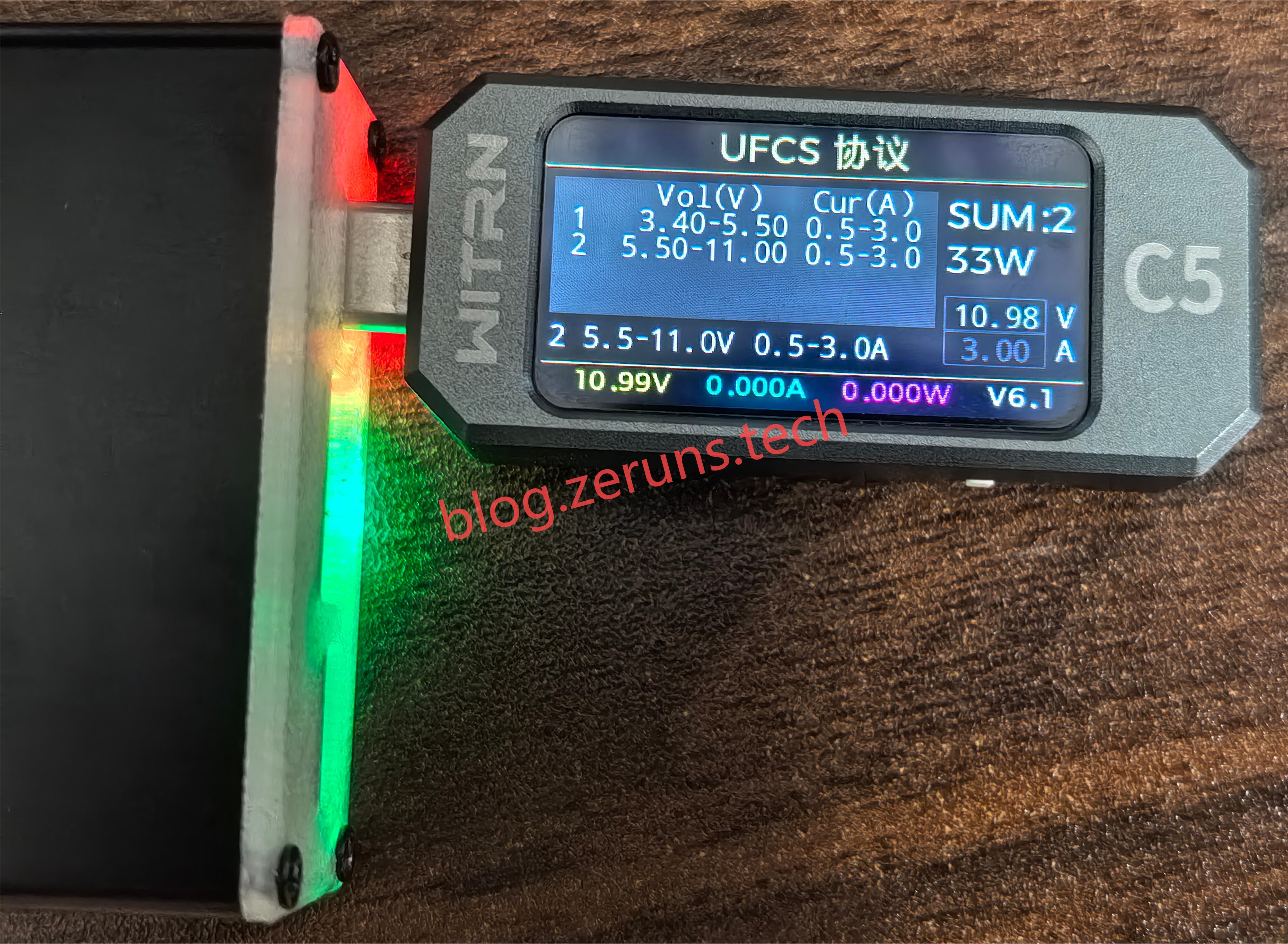
The C1 port also supports the UFCS protocol, though only up to 33W.
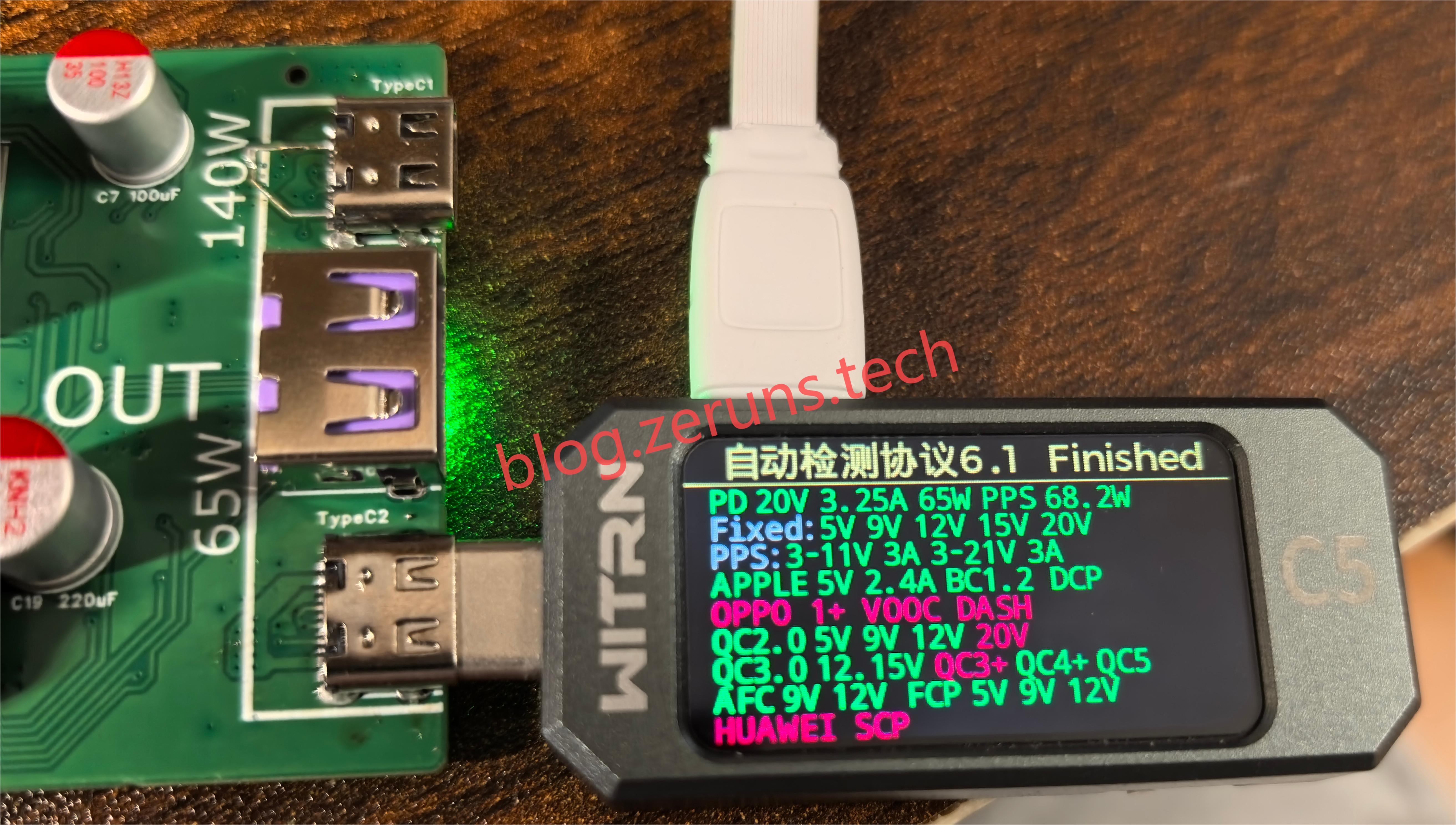
The protocols supported by the C2 port are shown below:
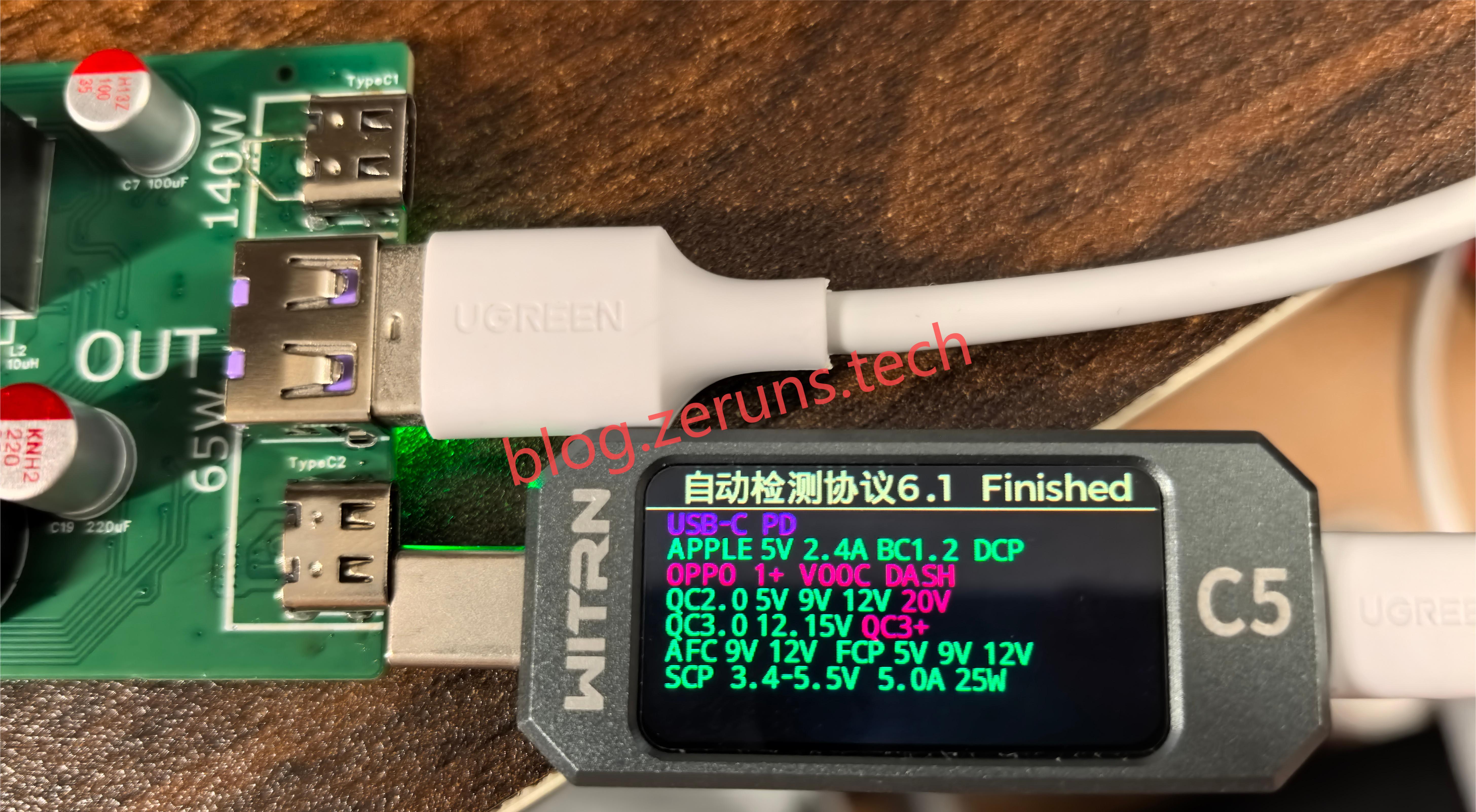
The protocols supported by the A port are shown below:
Output Load Testing
C1 Port Test
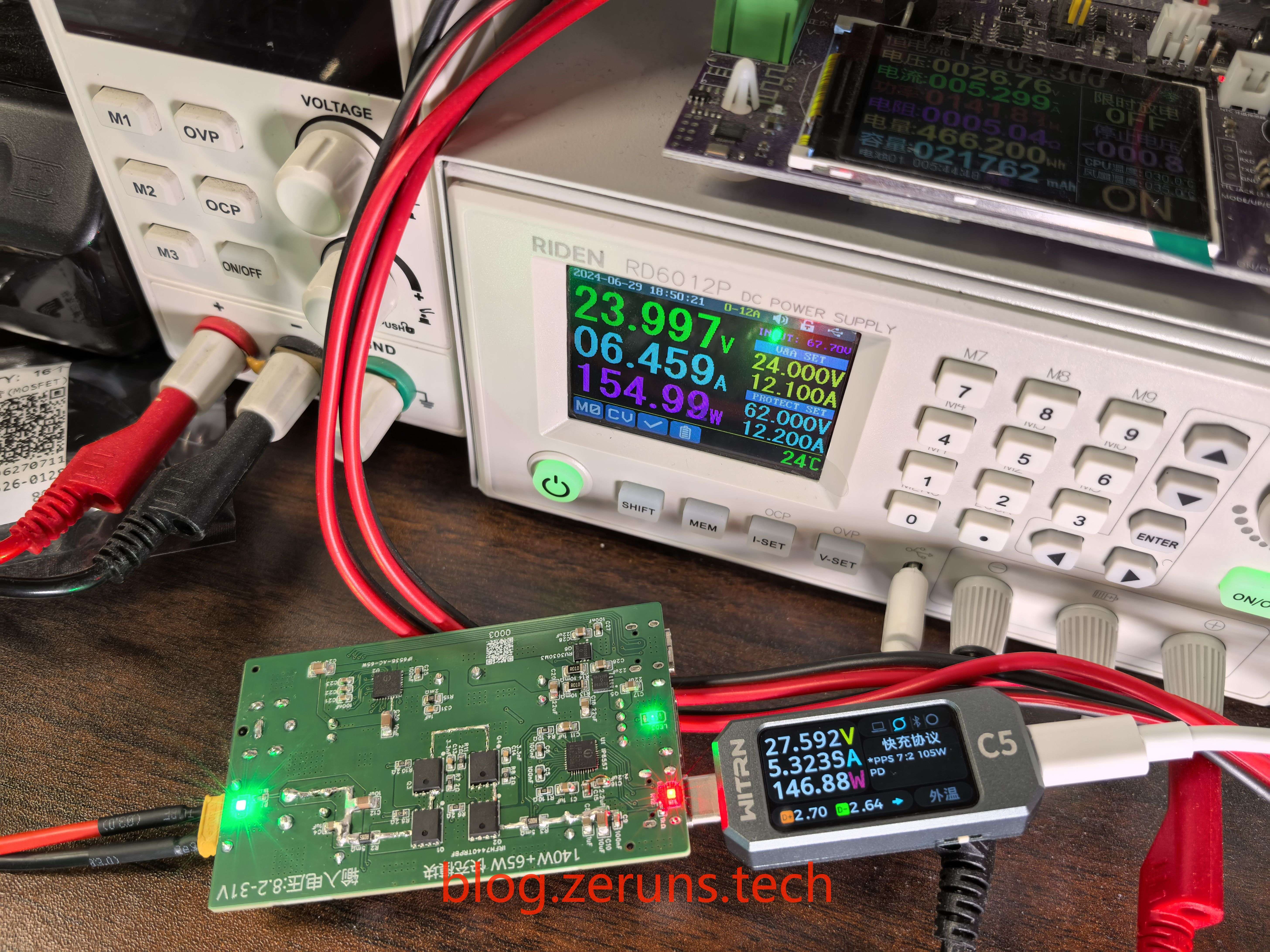
Using the XT30 interface, the input voltage was set to 24V, with the output spoofed to 28V and connected to an electronic load set to a current of 5.3A.
C2 Port Test
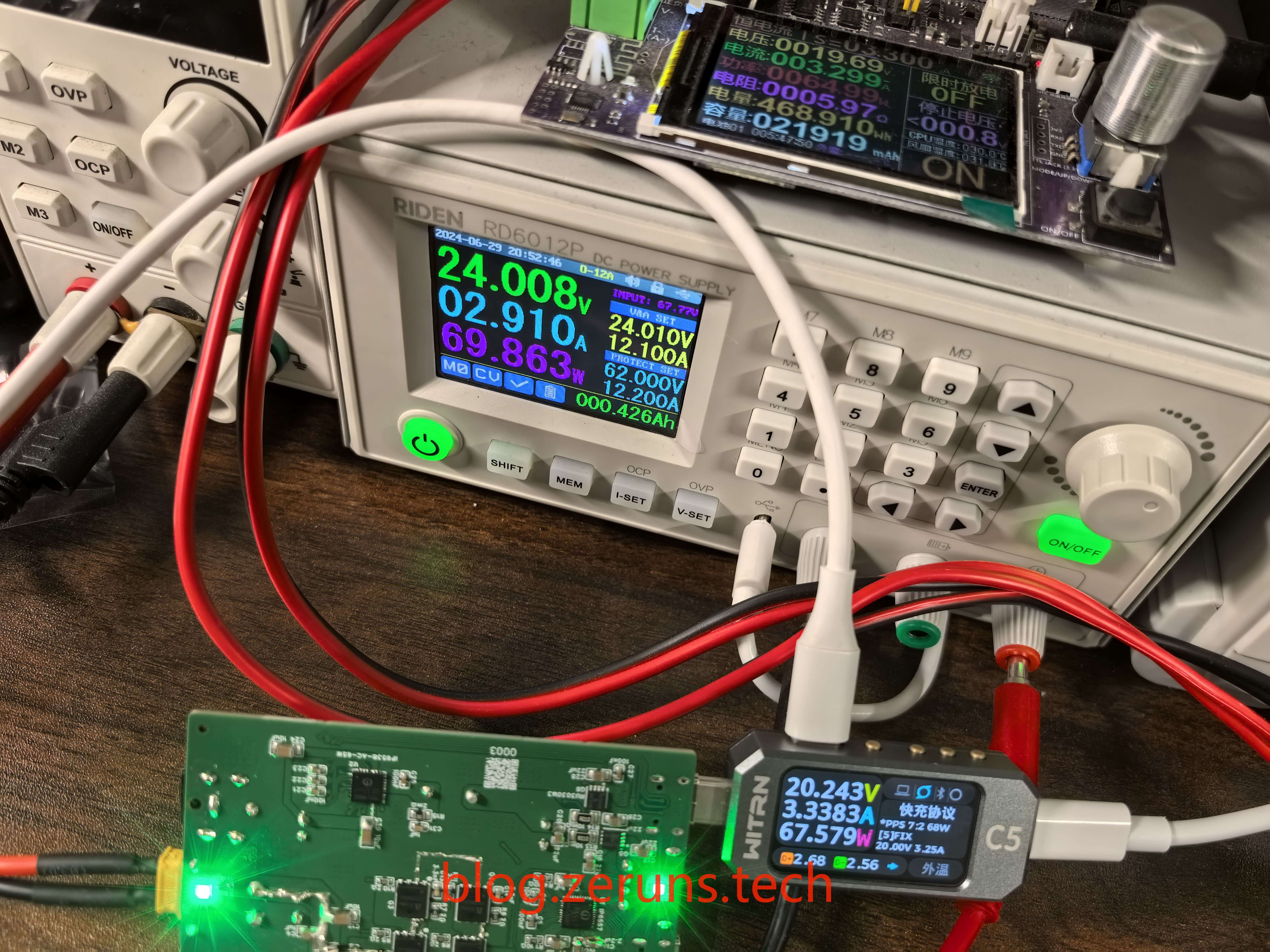
A Port Test
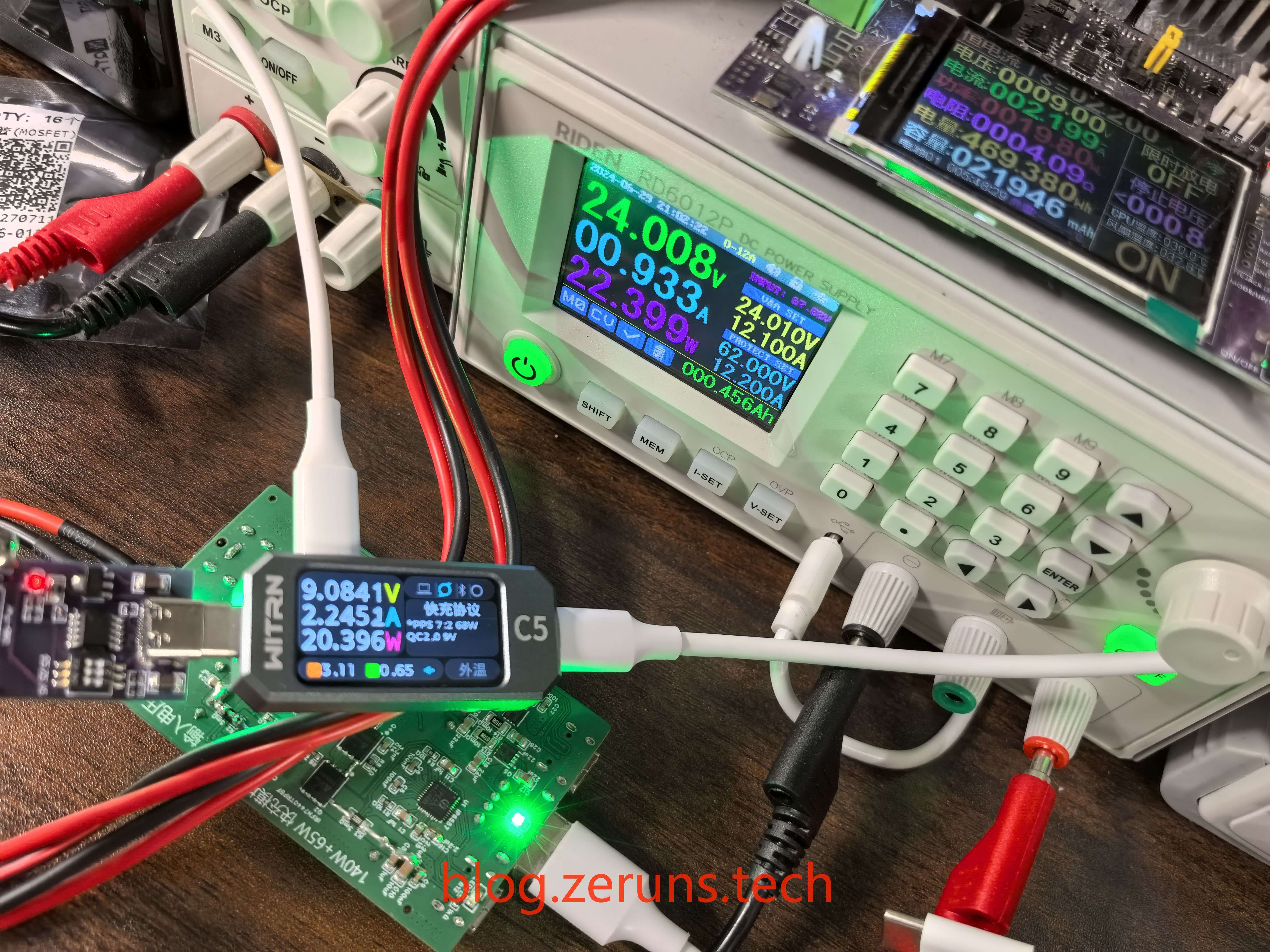
Dual-Port Full Load Test
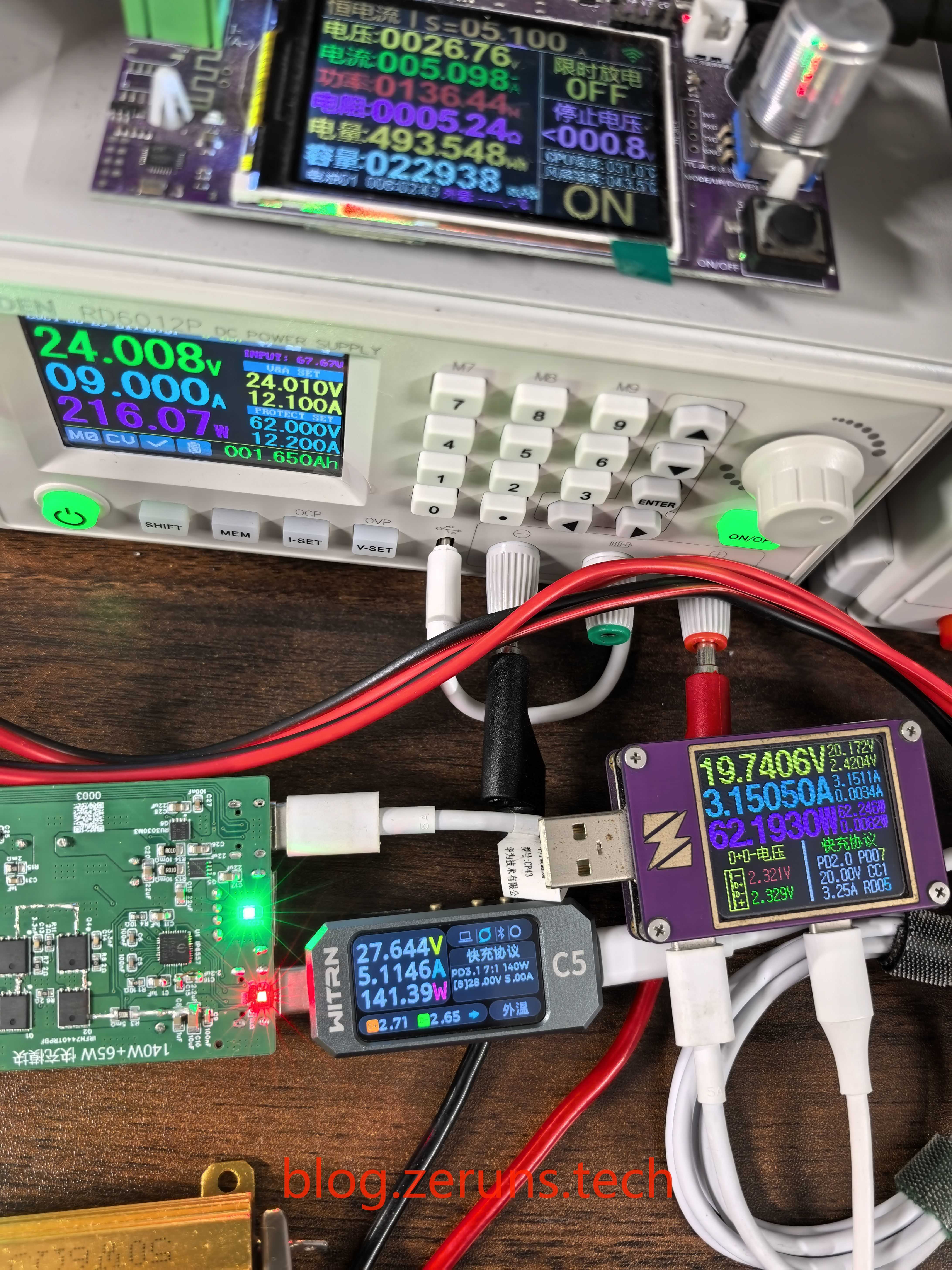
Equipment Used for Testing
- HP 34401A 6½-Digit Multimeter: https://blog.zeruns.tech/archives/772.html
- Riden RD6012P Programmable Power Supply: https://blog.zeruns.tech/archives/740.html
- Rigol DHO914S Oscilloscope: https://blog.zeruns.tech/archives/764.html
- 炬为电子负载:https://s.click.taobao.com/2sdCaht
- 优利德UTi261M热成像仪开箱测评:https://blog.zeruns.tech/archives/798.html
- WITRN维简C5检测仪(USB电压电流表/CC表):https://s.click.taobao.com/Sy2Daht
Conversion Efficiency Testing
The following tests measure efficiency under different input and output voltage conditions for both the C1 and C2 ports.
IP6557
Maximum conversion efficiency: 95.468%
| Input Voltage (V) | Input Current (A) | Input Power (W) | Output Voltage (V) | Output Current (A) | Output Power (W) | Conversion Efficiency (%) |
|---|---|---|---|---|---|---|
| 23.997 | 6.459 | 154.997 | 27.592 | 5.323 | 146.872 | 94.758 |
| 11.999 | 9.598 | 115.166 | 19.980 | 5.345 | 106.793 | 92.729 |
| 8.299 | 8.897 | 73.836 | 20.030 | 3.336 | 66.820 | 90.498 |
| 23.997 | 4.686 | 112.450 | 20.100 | 5.341 | 107.354 | 95.468 |
| 23.997 | 1.764 | 42.331 | 12.001 | 3.337 | 40.047 | 94.606 |
IP6538
Maximum conversion efficiency: 96.719%
| Input Voltage (V) | Input Current (A) | Input Power (W) | Output Voltage (V) | Output Current (A) | Output Power (W) | Conversion Efficiency (%) |
|---|---|---|---|---|---|---|
| 24.008 | 0.795 | 19.086 | 5.165 | 3.315 | 17.122 | 89.708 |
| 24.008 | 1.265 | 30.370 | 12.217 | 2.335 | 28.527 | 93.930 |
| 24.008 | 2.910 | 69.863 | 20.243 | 3.338 | 67.571 | 96.719 |
| 24.008 | 0.933 | 22.399 | 9.084 | 2.245 | 20.394 | 91.045 |
Thermal Performance and Infrared Imaging
C1 Port
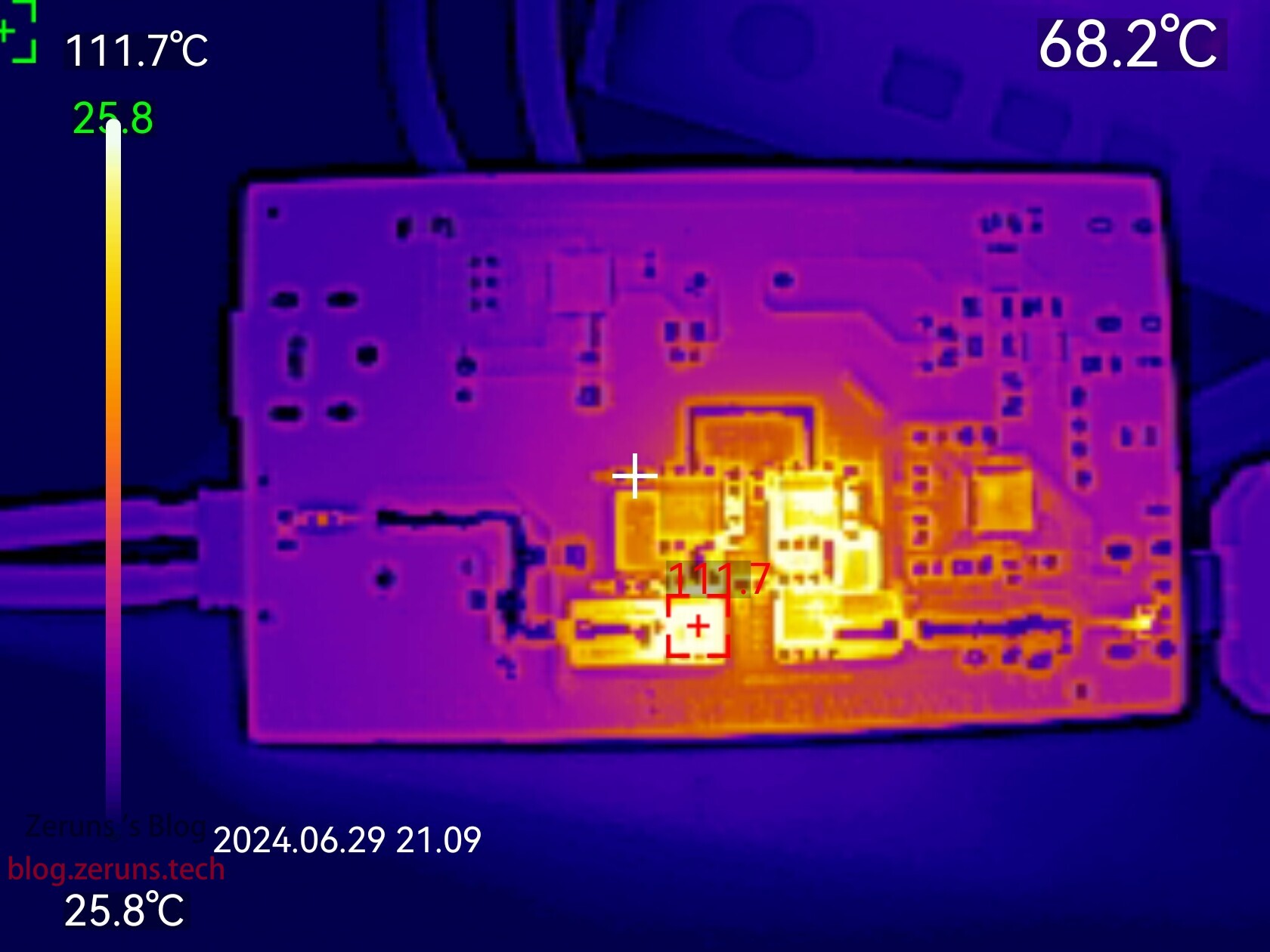
Infrared images of the PCB front and back after 5 minutes of 140W full-load output. The MOSFET temperature exceeded 111°C. For sustained full-load output, a heatsink or aluminum alloy enclosure is required, with a thermal pad to transfer heat to the enclosure.
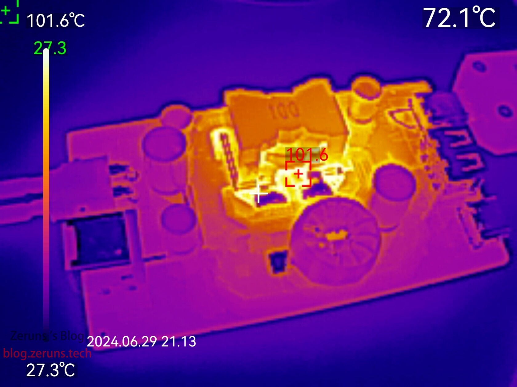
C2 Port
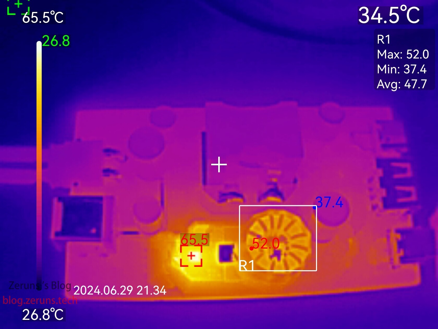
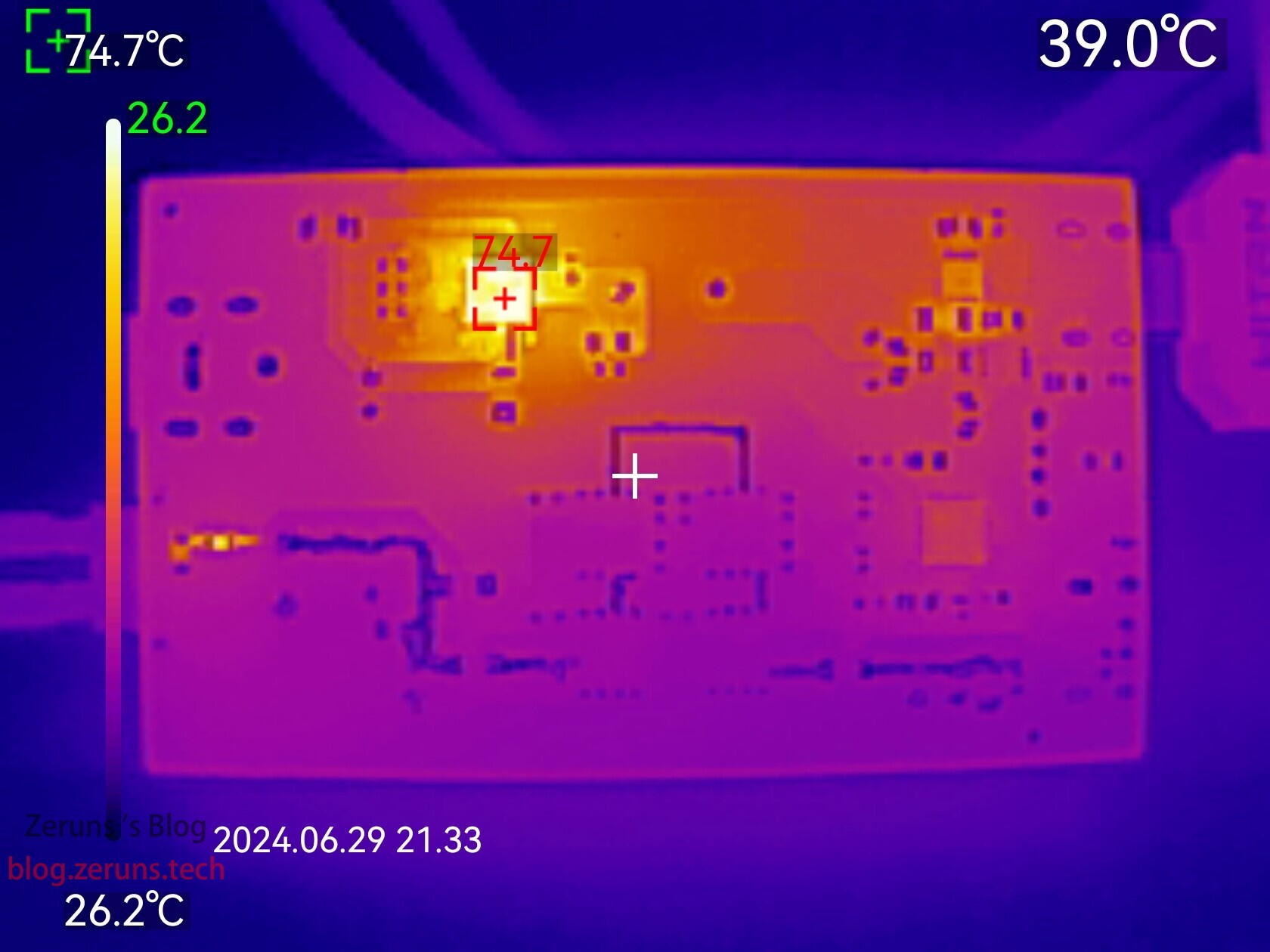
Infrared images of the PCB front and back after 10 minutes of 65W full-load output. The maximum temperature of the IP6538 chip was around 75°C, allowing for continuous full-load operation without a heatsink.
Dual-Port Full-Load Test
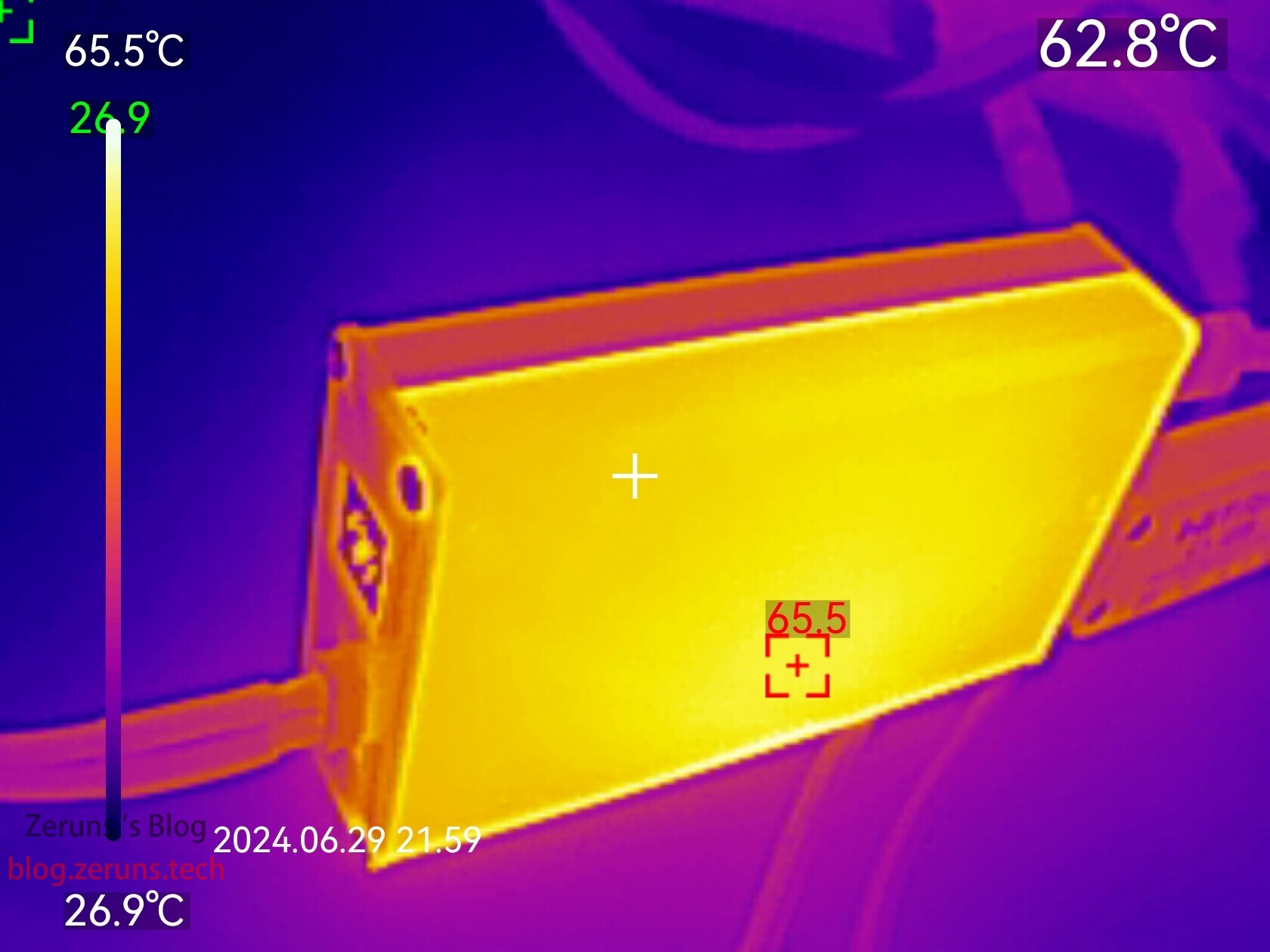
Infrared image of the aluminum alloy enclosure after 10 minutes of simultaneous full-load output. The maximum enclosure temperature was approximately 65°C. Due to the two-part design of the enclosure with a gap in the middle, heat was concentrated in the lower section.
Ripple Testing
The formula for calculating the ripple ratio is as follows:
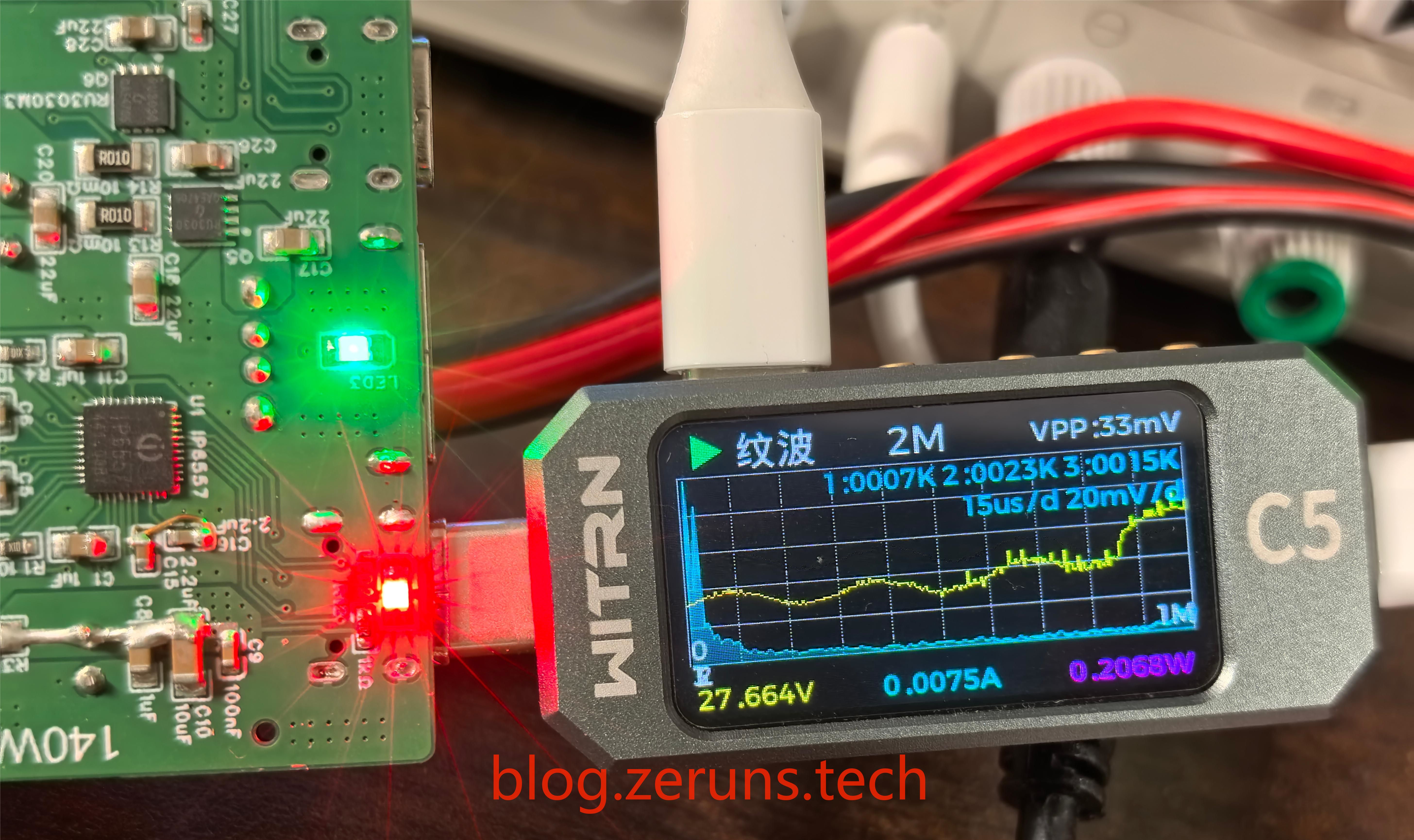
- When the C1 port outputs 28V (actual 27.6V), the ripple peak-to-peak value is approximately 33mV, with a ripple ratio of 0.059%.
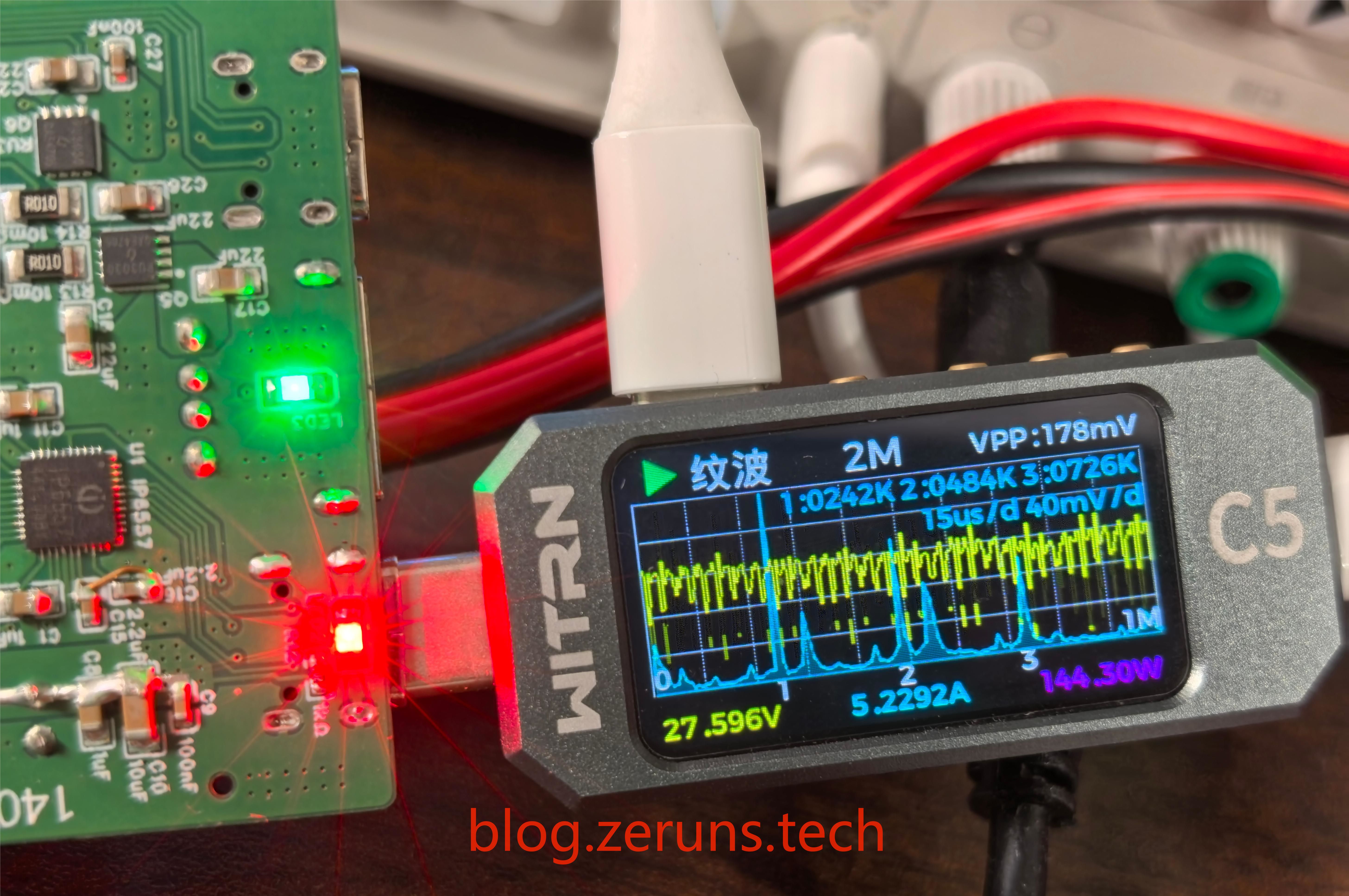
- When the C1 port outputs 28V at 5.2A, the ripple peak-to-peak value is approximately 178mV, with a ripple ratio of 0.323%.
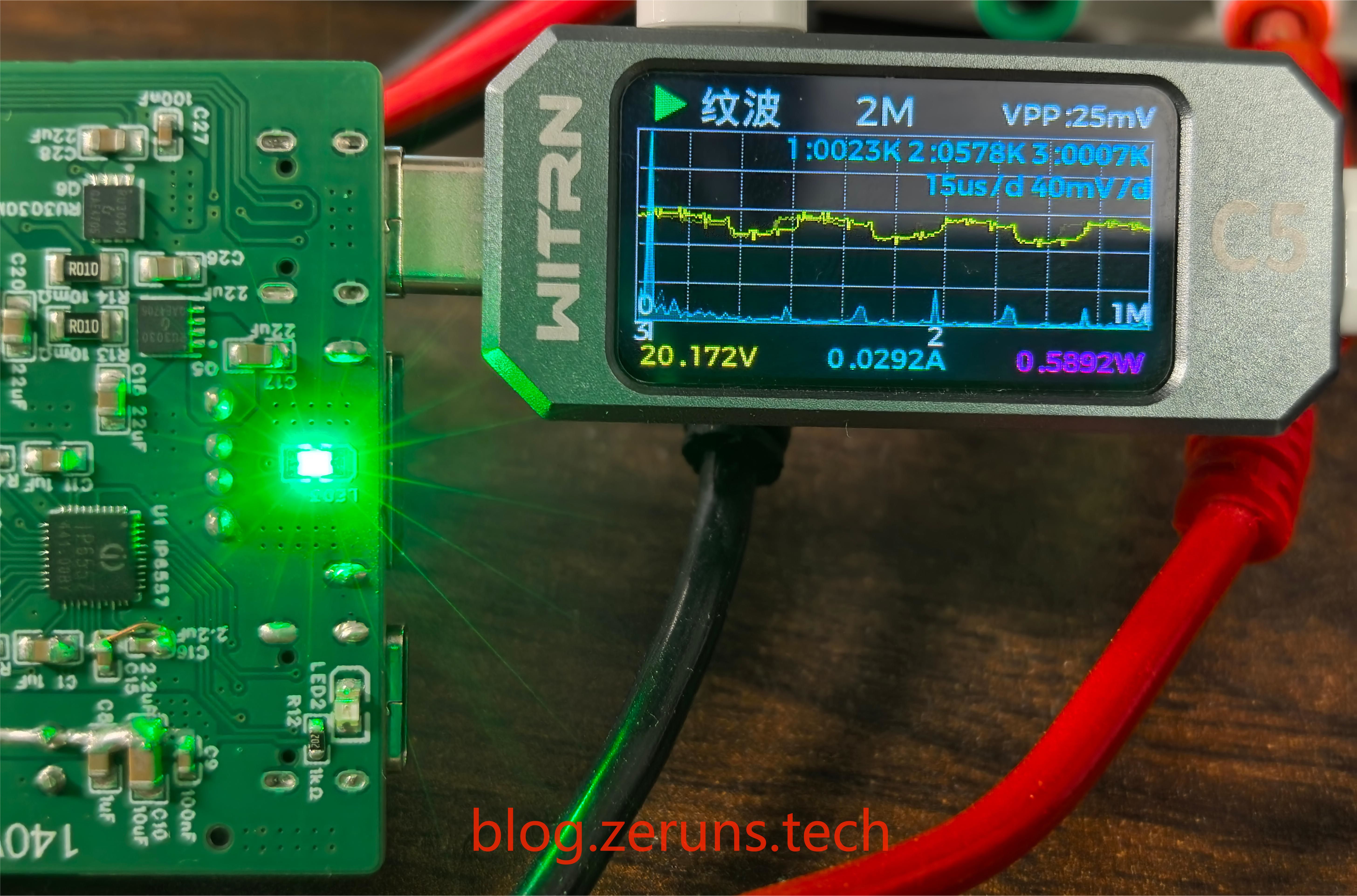
- When the C2 port outputs 20V with no load, the ripple peak-to-peak value is approximately 25mV, with a ripple ratio of 0.062%.
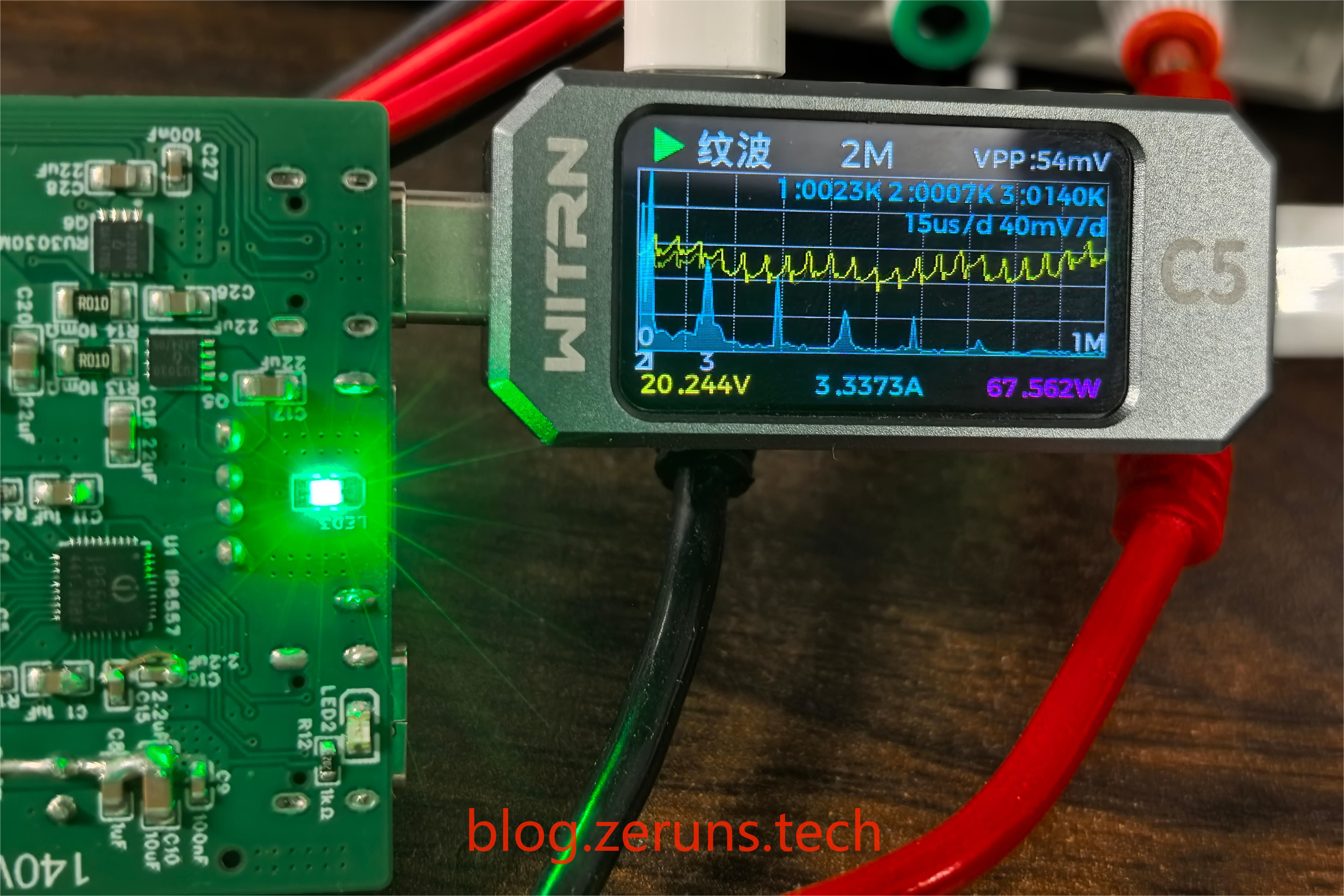
- When the C2 port outputs 20V at 3.3A, the ripple peak-to-peak value is approximately 54mV, with a ripple ratio of 0.133%.
The ripple performance is satisfactory.
Circuit Diagram
IP6557:
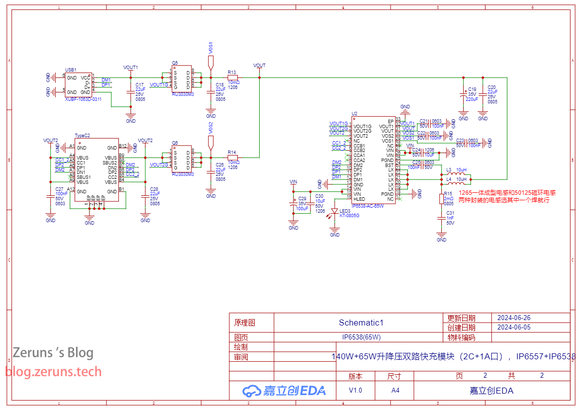
IP6538:
PCB
Top Layer:

Bottom Layer:

Component Purchase Links
The purchase links for most of the components used in this project can be found here:
- 0603电阻电容样品本:https://s.click.taobao.com/XXCyZht
- TypeC母座 16P:https://s.click.taobao.com/6HYxZht
- IP6557芯片:https://s.click.taobao.com/Jor7Fit
- IP6538芯片:https://s.click.taobao.com/aPw6Fit
- AGM405Q MOS管:https://s.click.taobao.com/0aR6Fit
- XT30PW-M接口:https://s.click.taobao.com/cPB6Fit
- 扁平线电感PQ2012 10μH:https://s.click.taobao.com/SoguZht
- 50125磁环电感 卧式 10μH 10A:https://s.click.taobao.com/B6quZht
- 35V 220μF固态电容:https://s.click.taobao.com/CxL3Fit
- 35V 100μF固态电容:https://s.click.taobao.com/z9FtZht
- 铝合金外壳:https://s.click.taobao.com/xmRkZht
It is suggested to purchase components from LCSC Mall:
https://activity.szlcsc.com/invite/D03E5B9CEAAE70A4.html
You can directly import the required components into your shopping cart by clicking “Order Now” in the BOM table from the LCSC Open Source link.
Resource Download Links
The following download links contain the LCSC EDA project, schematic PDF files, datasheets of the chips used, and 3D model files for the enclosure.
- Baidu Netdisk Download Link:
https://pan.baidu.com/s/1RJNC_v2P1YijWpv1sFXowQ?pwd=89hi
Access Code: 89hi - 123 Cloud Disk Download Link:
https://www.123pan.com/s/2Y9Djv-BItvH.html
Access Code: 0nEm
If you find these resources helpful, you can send a donation via the 123 Cloud Disk link above. Alternatively, if this is a WeChat article (WeChat public account: zeruns-gzh), you can use the "Like Author" feature at the bottom of the article to support me. Thank you!
Other Open-Source Projects to Explore
- A Three-Phase Electricity Collector for Home Energy Monitoring:
https://blog.zeruns.tech/archives/771.html - LVGL Project Template Based on STM32F407 (MSP3526 Screen), Includes FreeRTOS and Bare Metal Versions:
https://blog.zeruns.tech/archives/788.html - Open-Source Synchronous Rectification Buck-Boost Digital Power Supply Based on STM32:
https://blog.zeruns.tech/archives/791.html - LM25118 Auto Buck-Boost Adjustable DC-DC Power Module:
https://blog.zeruns.tech/archives/727.html - EG1164 High-Power Synchronous Rectification Boost Module, Efficiency up to 97%:
https://blog.zeruns.tech/archives/730.html - 4G Environmental Monitoring Node Based on Air700E (Temperature, Humidity, Pressure, etc.), Uploading to Alibaba Cloud IoT via MQTT:
https://blog.zeruns.tech/archives/747.html - Open-Source Intelligent Electronic Load Based on CH32V307 (Embedded Competition Project):
https://blog.zeruns.tech/archives/785.html - EG1151 High-Power Adjustable Buck-Boost Module (Supports Type-C PD Fast Charging Input):
https://blog.zeruns.tech/archives/794.html
Recommended Reads
- High-Performance and Affordable VPS/Cloud Server Recommendations:
https://blog.zeruns.tech/archives/383.html - Minecraft Server Setup Guide:
https://blog.zeruns.tech/tag/mc/ - No-Code Blog Setup Guide! A Comprehensive Guide to Building a Personal Blog:
https://blog.zeruns.tech/archives/783.html - Intranet Penetration Server Setup Guide, NPS Deployment and Usage Tutorial:
https://blog.zeruns.tech/archives/741.html - Raincloud Ningbo 8272CL High-Bandwidth, High-Defense Cloud Server Review, Up to 500Mbps Bandwidth and 1TB Cloud Disk:
https://blog.zeruns.tech/archives/789.html - Testing and Teardown of a 120W Charger Purchased for Only ¥2.6 on Douyin Mall:
https://blog.zeruns.tech/archives/786.html


Comment Section