


Open-sourcing a USB3.2 expansion dock with Type-C input: 4 USB3.2 Gen2 ports + 2.5G Ethernet + TF/SD card readers, supports PD fast charging for auxiliary power, input voltage range 4 to 20 V, Buck-Boost circuit regulating output to 5.1 V, based on VL160 + VL822 + RTL8156BG + GL3224 chips.
Open-Source USB 10 Gbps Hub with 2.5 Gbps Ethernet & TF/SD Card Reader
📍I've never undertaken a high-speed PCB project like this before—it's my first time. Any suggestions for improvements or pointing out mistakes would be greatly appreciated.
🚀By the way, I'm currently job hunting online. If any employers in Guangzhou or Foshan are hiring, please consider me. You can check out my open-source projects on my OSHWHub profile: https://oshwhub.com/zeruns/works
▶Project demonstration & design process videos: https://www.bilibili.com/video/BV145G1z9Em2/
▶Open-source repository on OSHWHub: https://url.zeruns.com/U9sCt
▶Electronics/Microcontroller Tech QQ Group: 2169025065
Download links are at the end of the article!
Project Overview
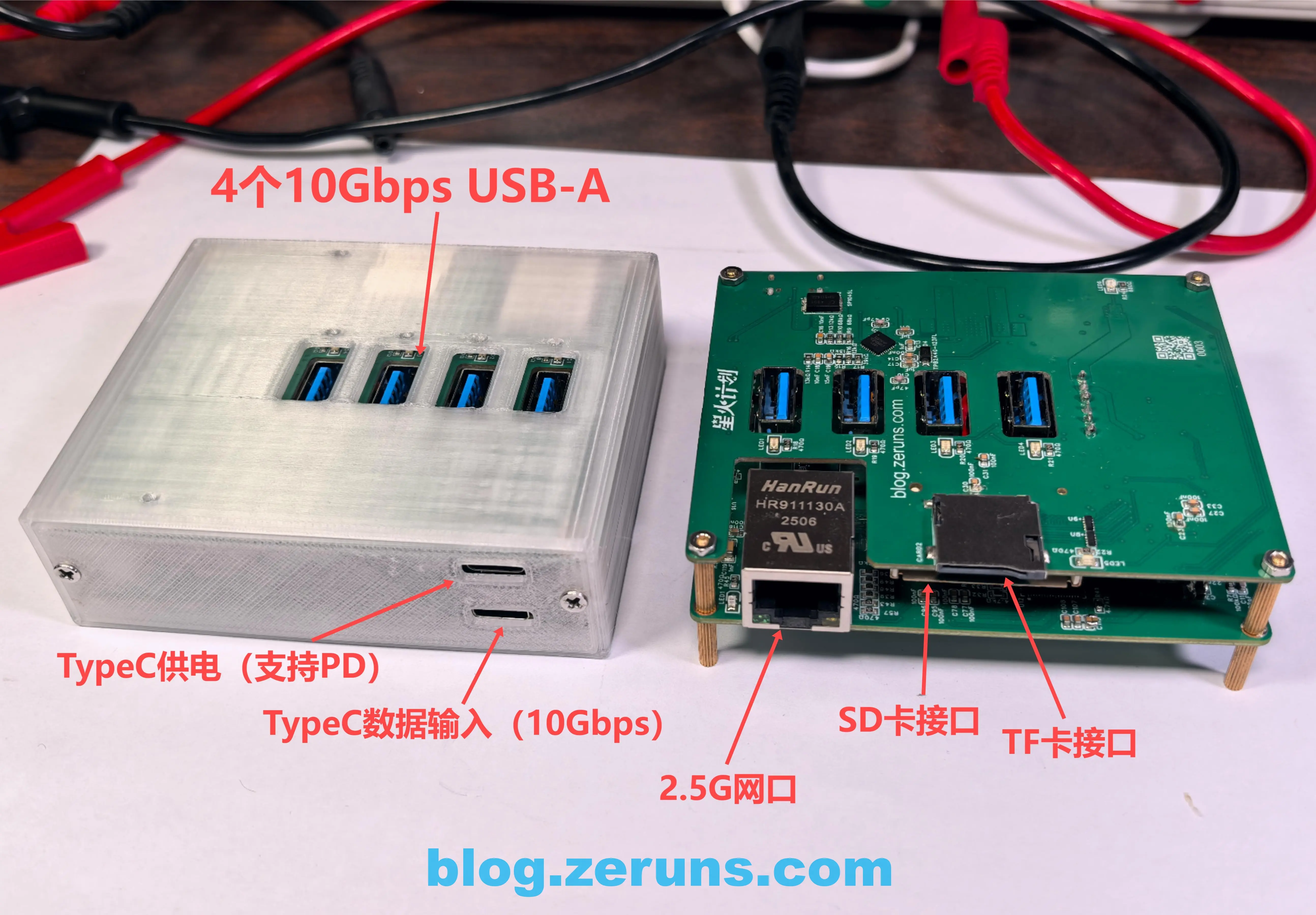
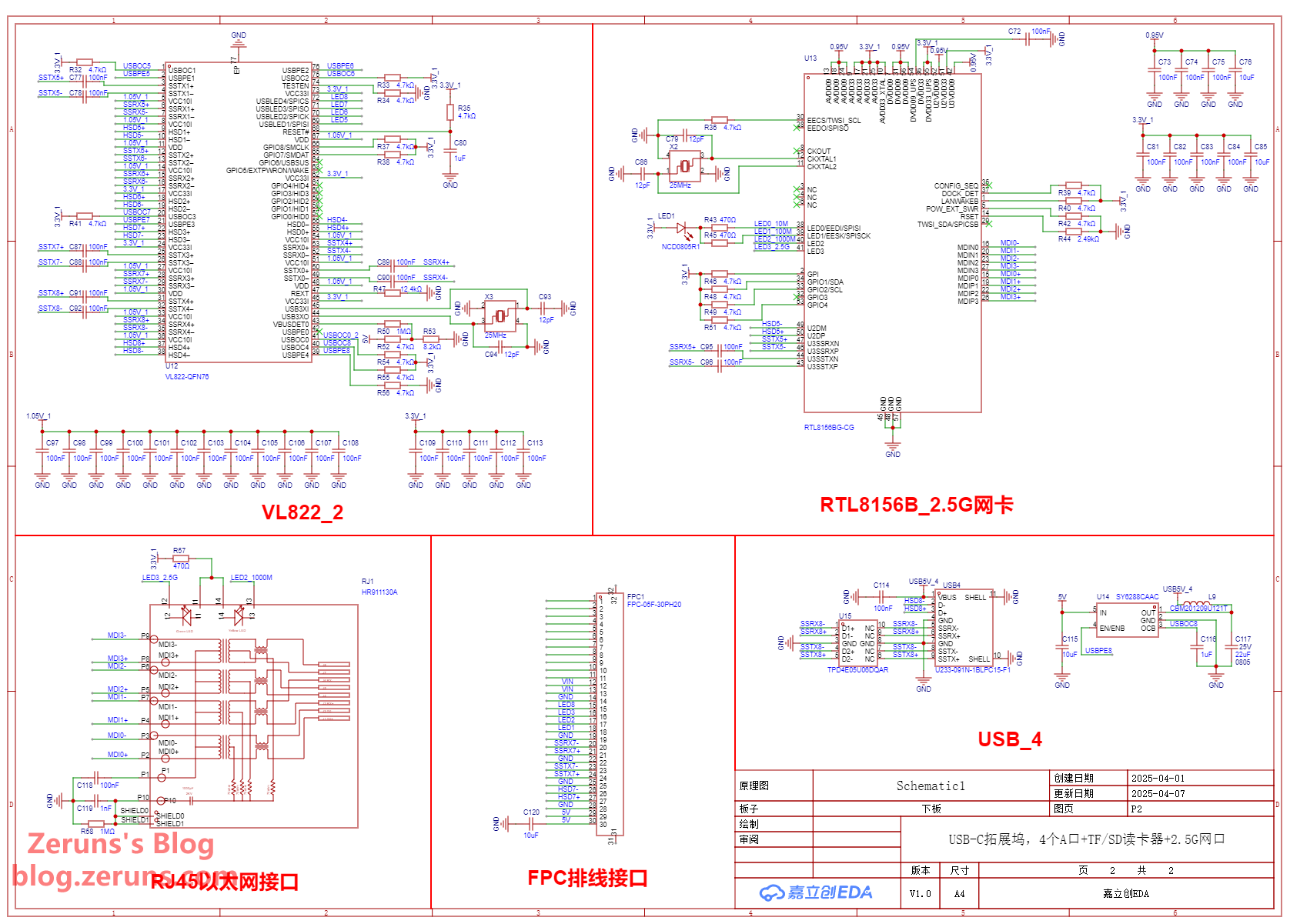
▶This is a USB3.2 expansion dock with a USB-C input, featuring four USB3.2 (10 Gbps) Type-A outputs (the input port is also 10 Gbps, so total throughput remains 10 Gbps), plus one 2.5 G Ethernet port and TF/SD card readers.
▶The 5 V power supply section uses a Buck-Boost converter to regulate output to 5.1 V (the extra 0.1 V compensates for voltage drop under high current). There are two Type-C inputs: one is a data port (also accepts power but doesn't trigger fast charging—it only accepts 5 V and is routed through the converter to prevent voltage sag under heavy load), and the other is a power port (supports PD fast charging by negotiating 20 V output, then stepping down via the converter to 5.1 V). The 5 V supply can deliver up to 9.5 A in total, with each USB-A port supporting up to 2 A.
▶This project employs two VL822 chips; one still has an unused USB interface that you could repurpose—for example, by adding another Type-A output, or integrating a microcontroller with voltage/current sensing to capture real-time power metrics on each USB port and relay them to a host PC via USB. This is useful for embedded debugging or power monitoring of USB devices (which was my initial plan, but I omitted due to PCB size constraints and to avoid making the board too large).
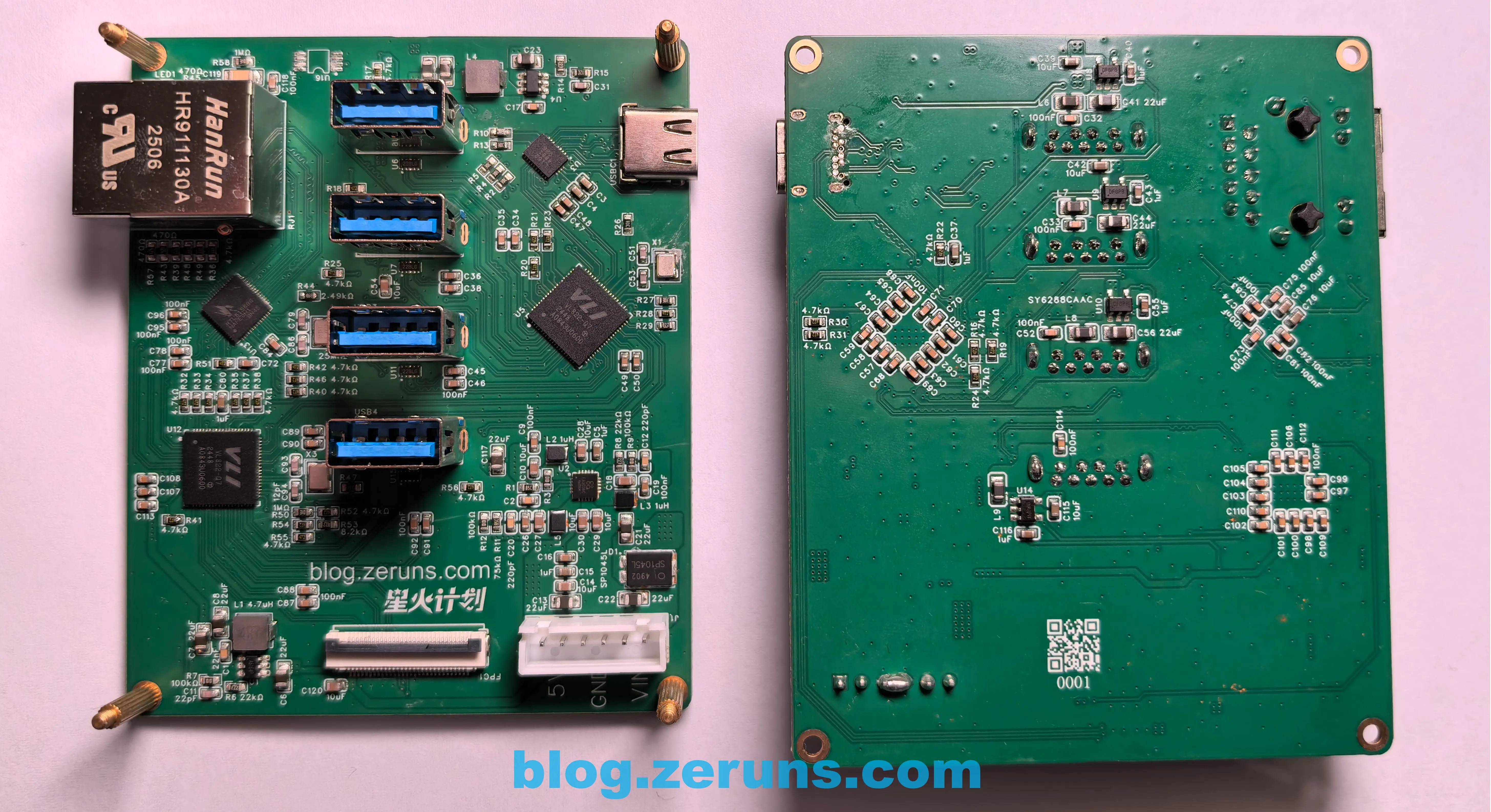
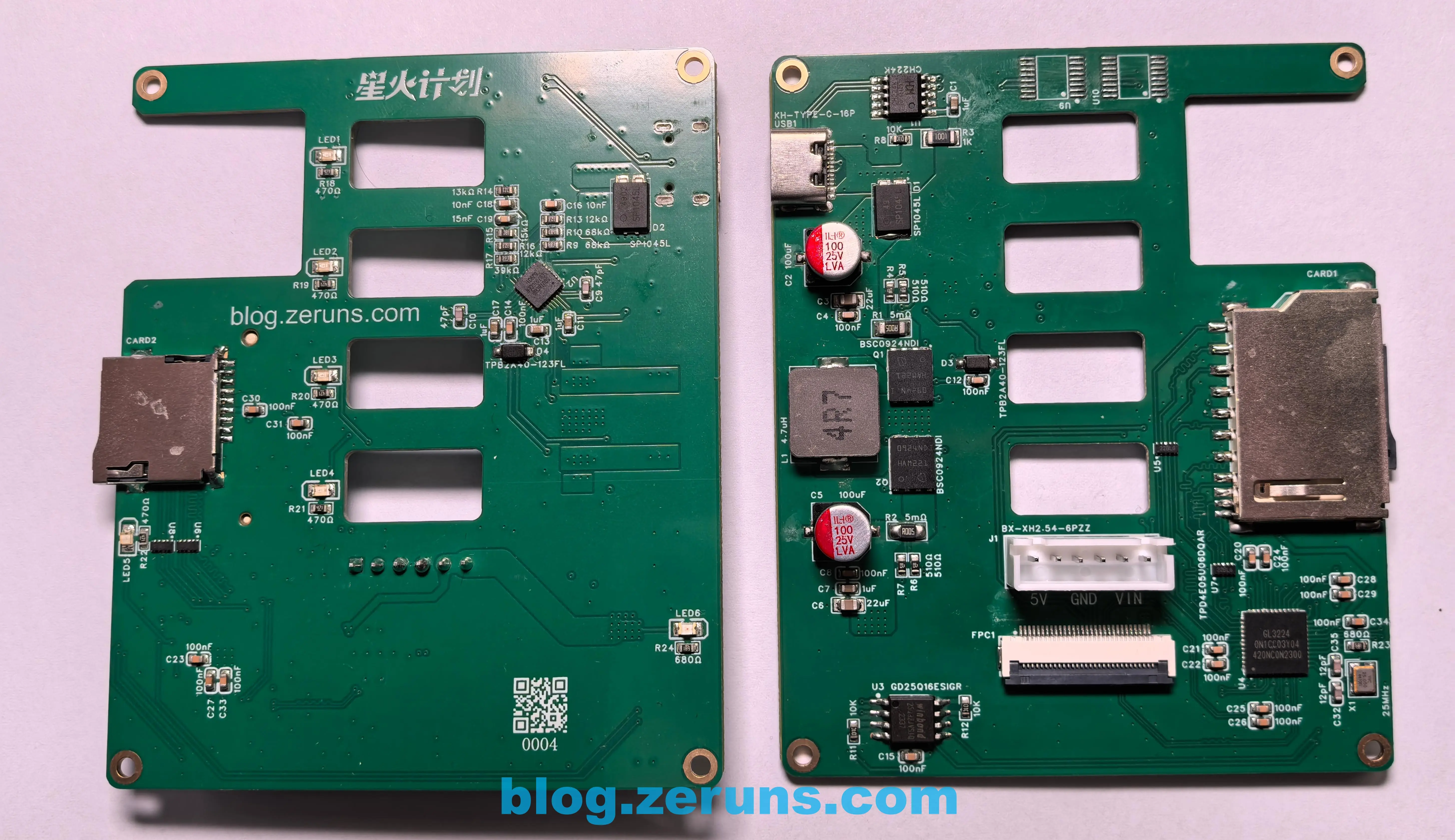
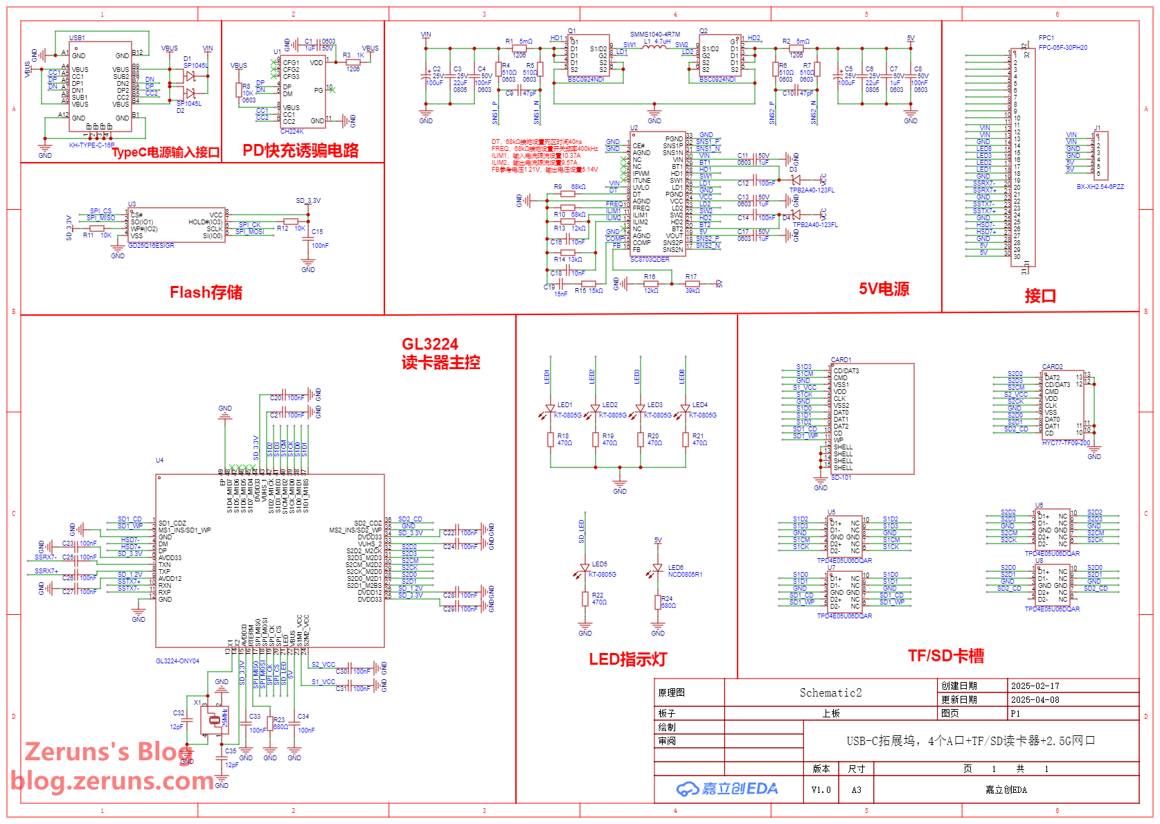
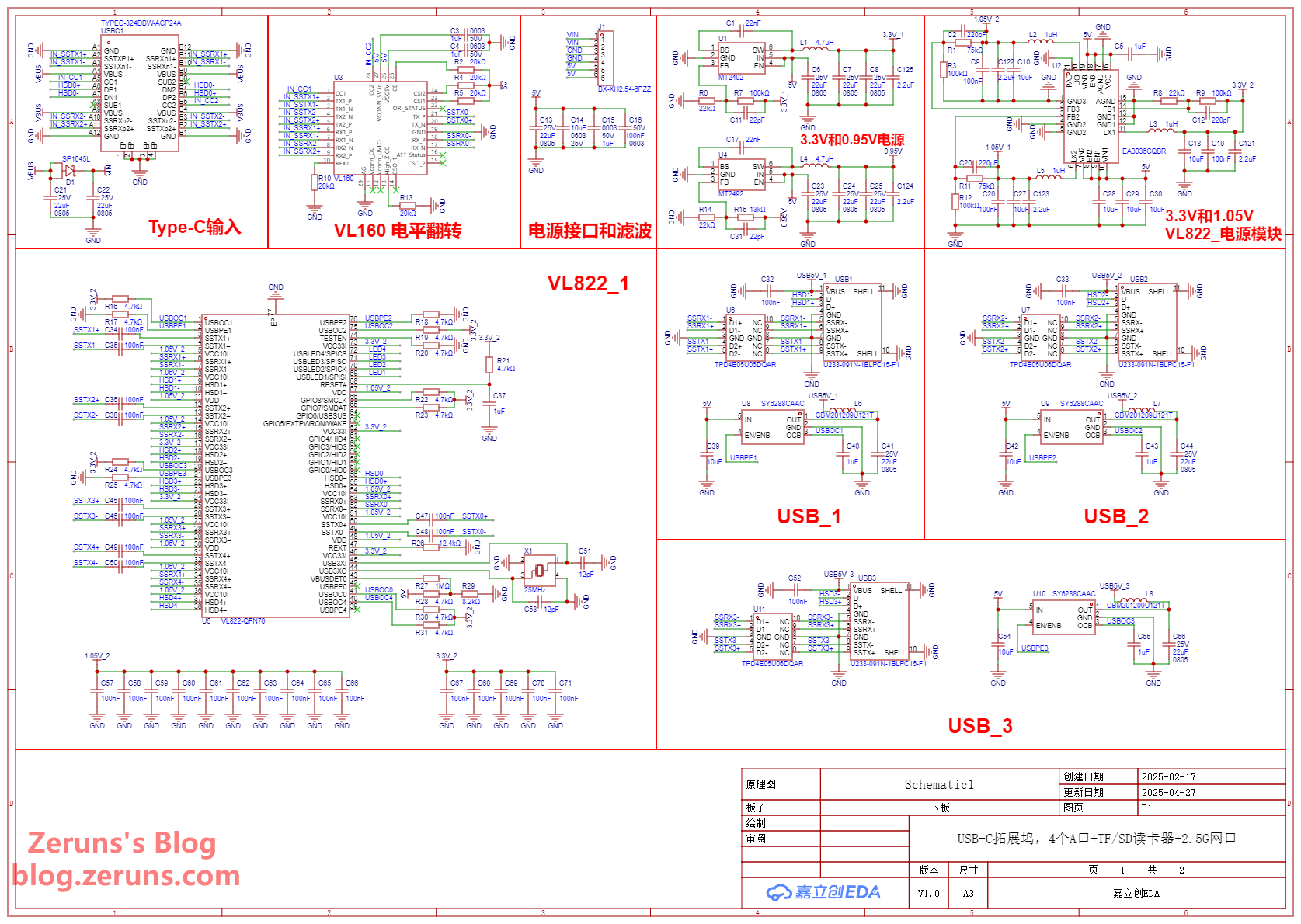
▶The design is split into two boards: the upper board houses the 5 V Buck-Boost power circuit and the card reader circuitry, while the lower board contains the USB hub and 2.5 G Ethernet circuitry. The boards connect via an FPC cable and XH2.54 headers.
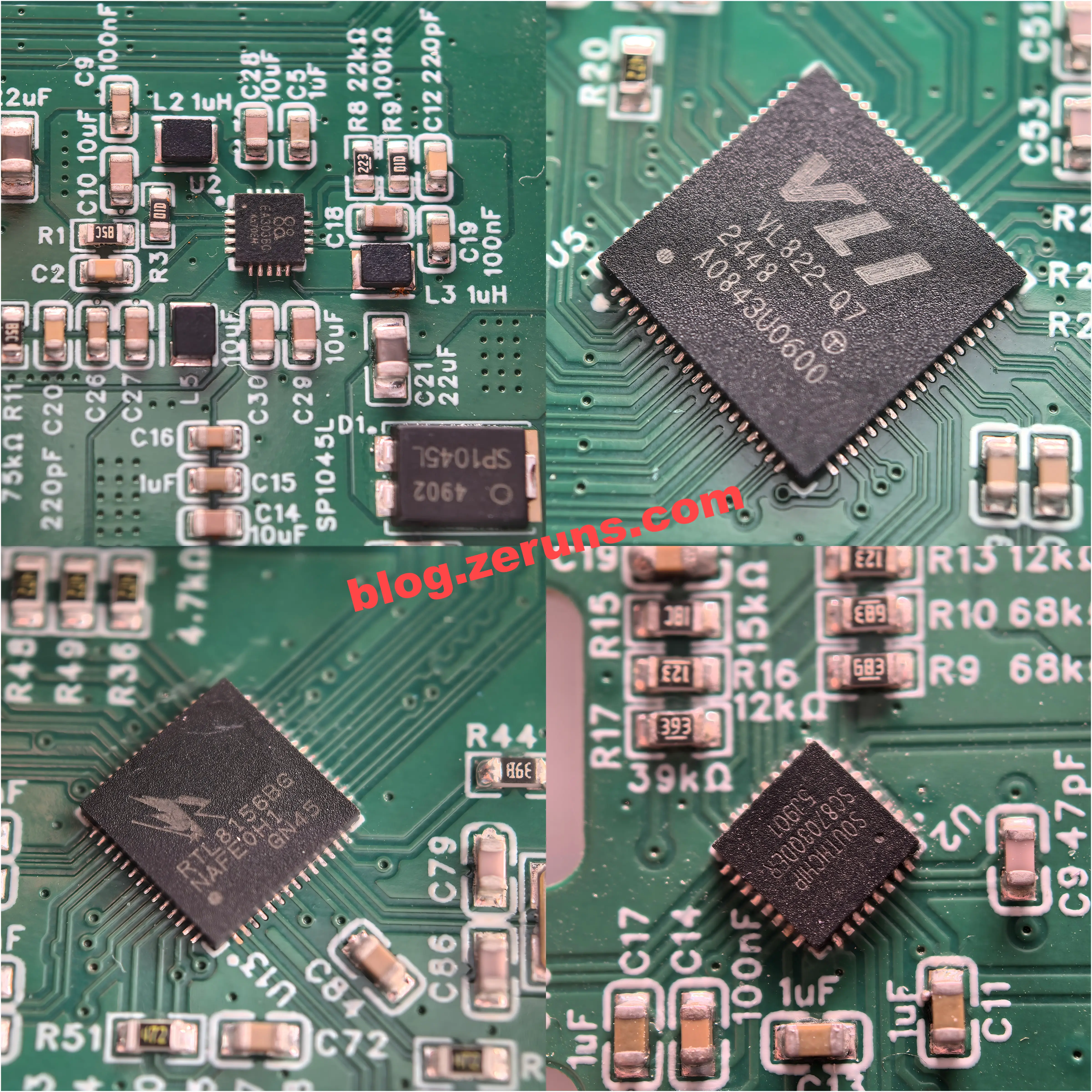
▶Key chips used: VL160, VL822, RTL8156BG, GL3224, EA3036, MT2492, SC8703
▶This design references the project “USB3 docking station with independent voltage regulation”: https://oshwhub.com/leo_lin/usb3-dock-with-dc-dc-converter
Expansion Dock Specifications
- Input Interface: USB-C
- Output Interfaces: USB-A, RJ45, TF, SD
- Maximum Input Data Rate: 10 Gbps
- Maximum Output Data Rates: USB: 10 Gbps | RJ45: 2.5 Gbps
- Type-C Maximum Input Power: 5 V@5 A / 20 V@5 A
- Type-A Maximum Output Current: 5 V@2 A (total across all ports up to 8 A)
- Dimensions: 90 × 74 × 26.3 mm
Product Photo
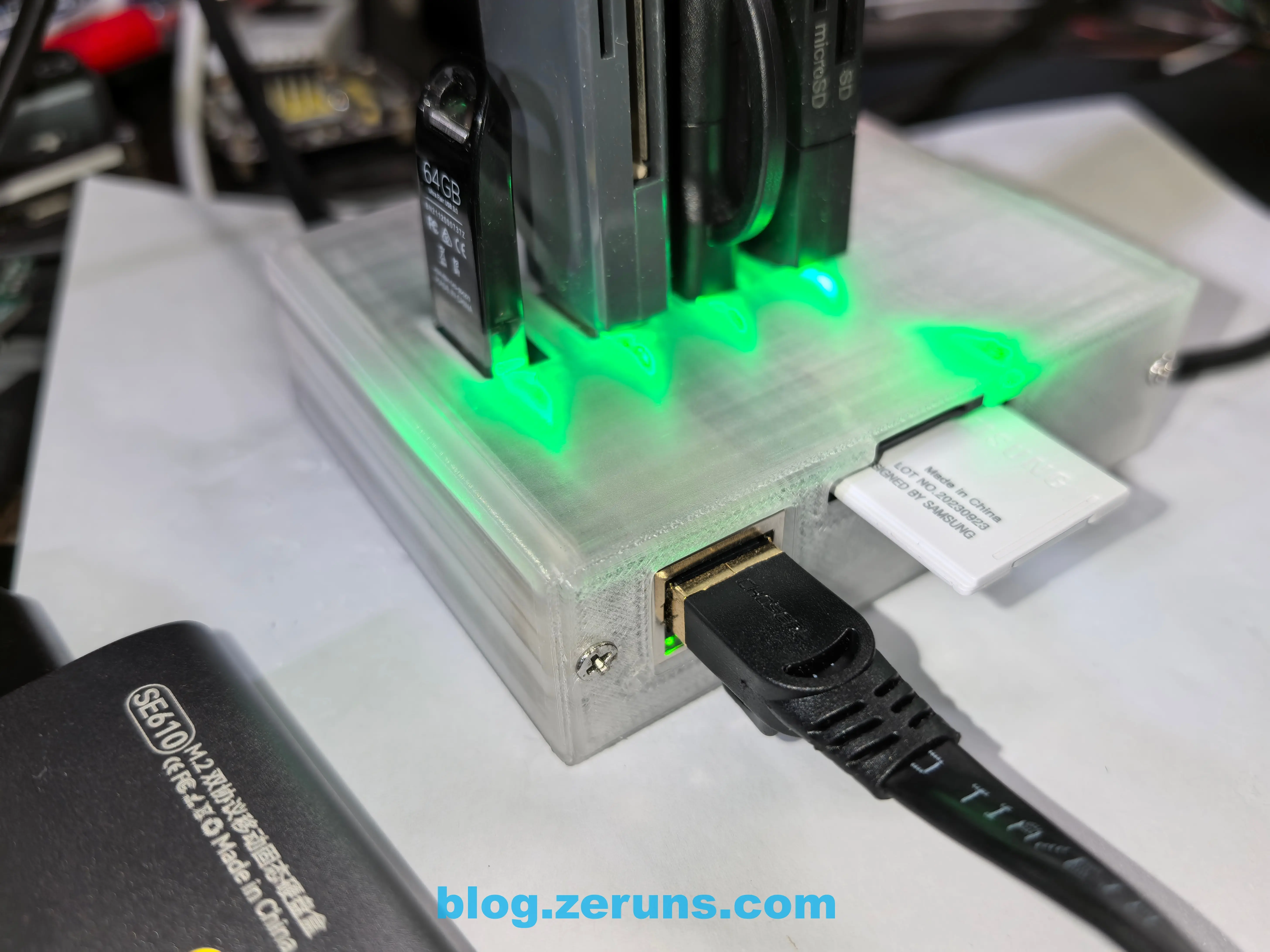
With the enclosure installed
Powered on and in operation
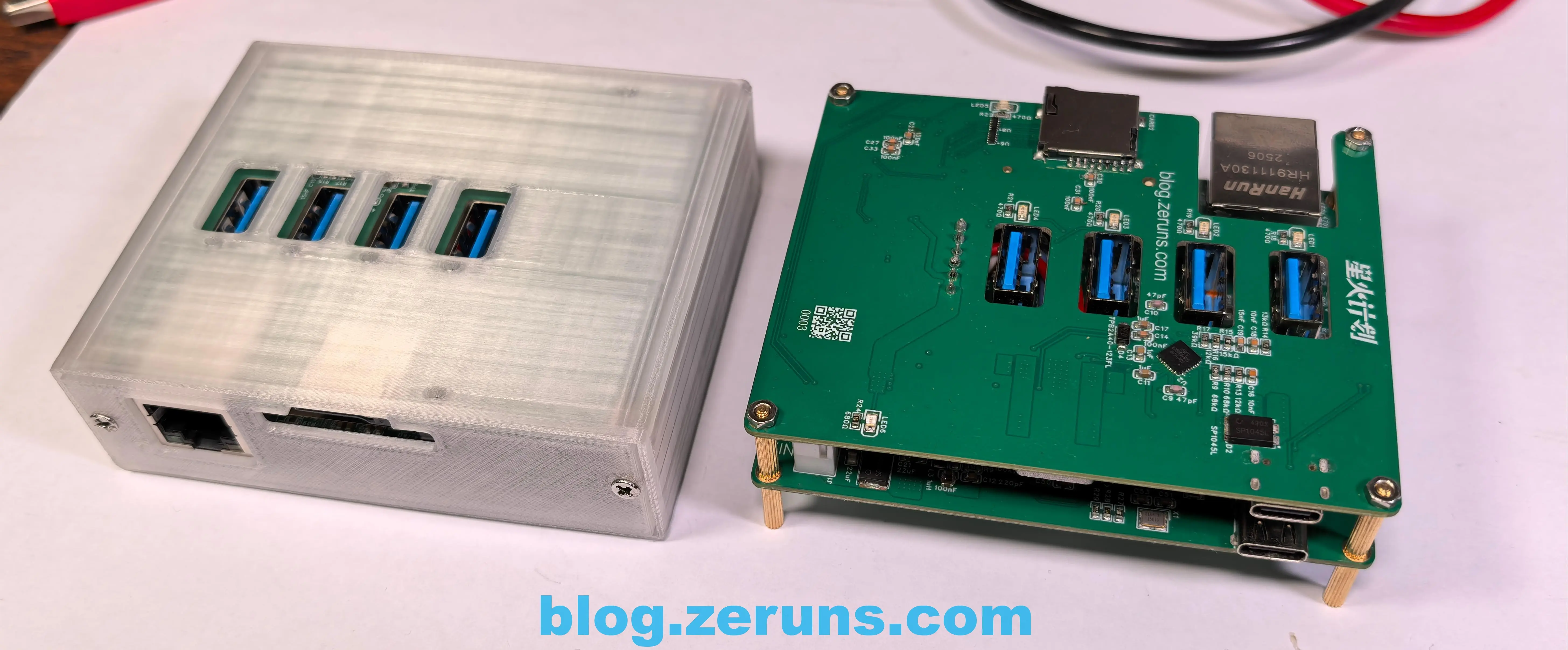
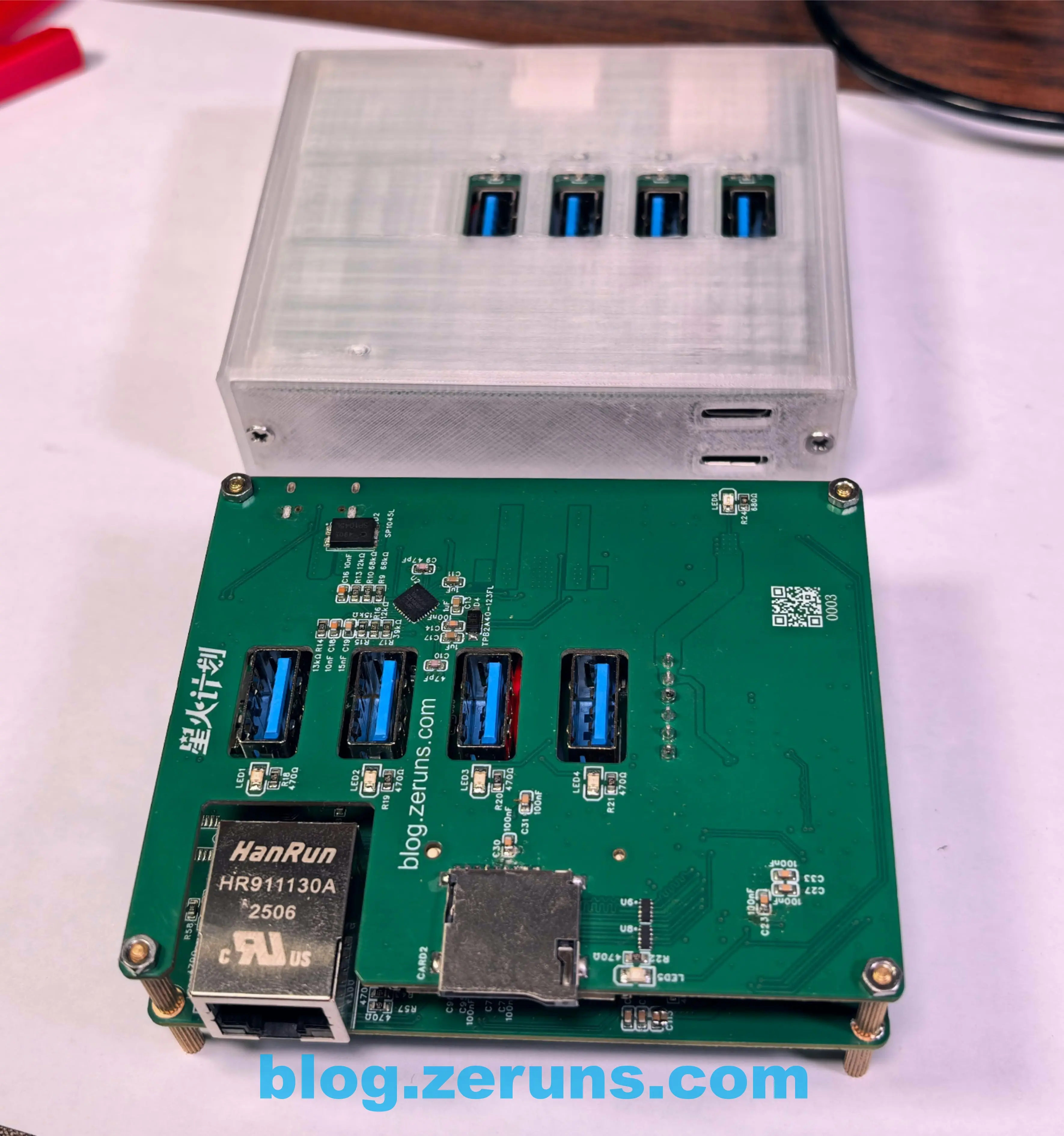
Circuit board
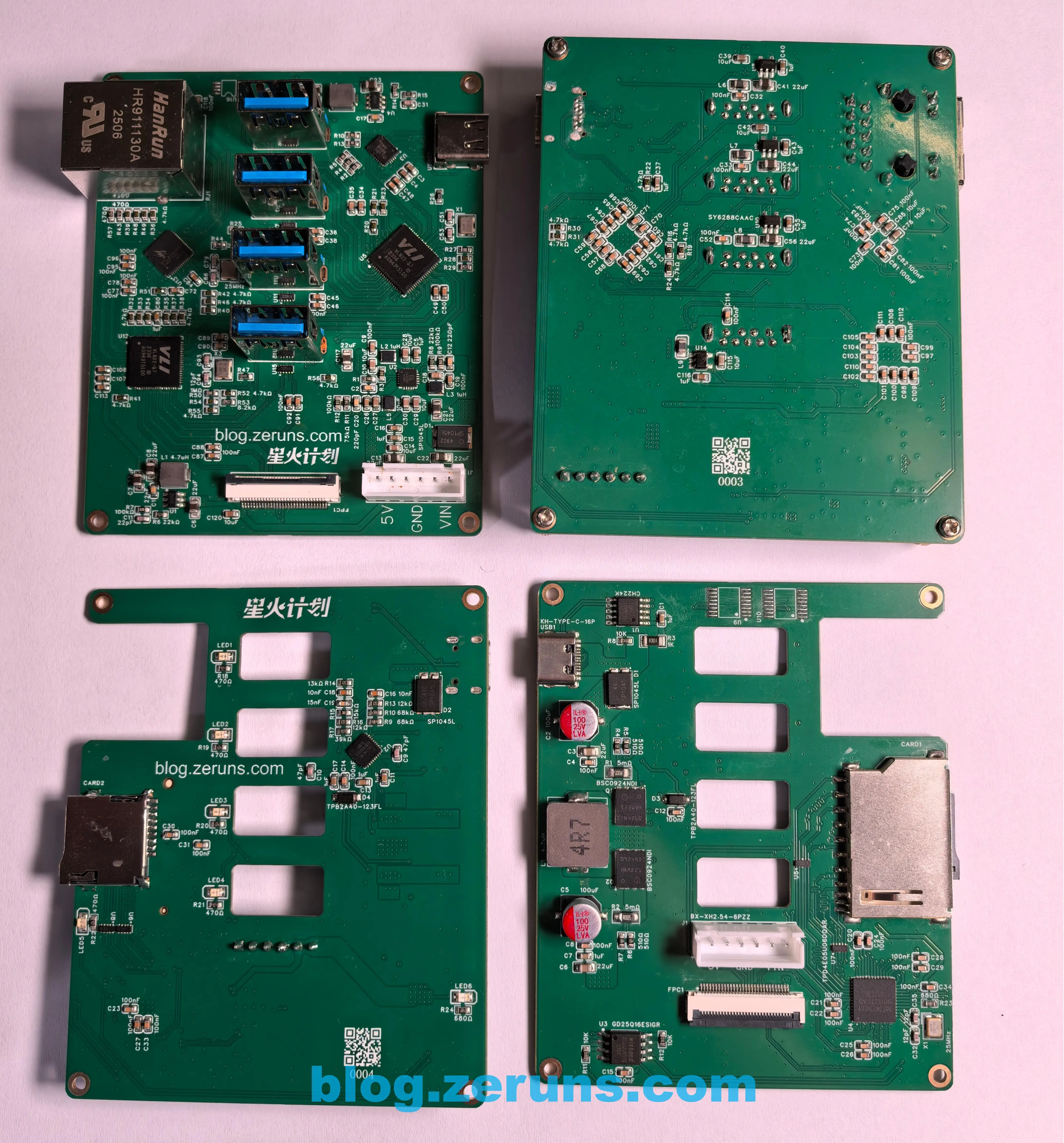
Bottom board, front and back
Top board, front and back
Hardware Implementation
When the user connects the expansion dock to a USB interface at 5 Gbps or higher,
High-Speed Bus Hardware Block Diagram:
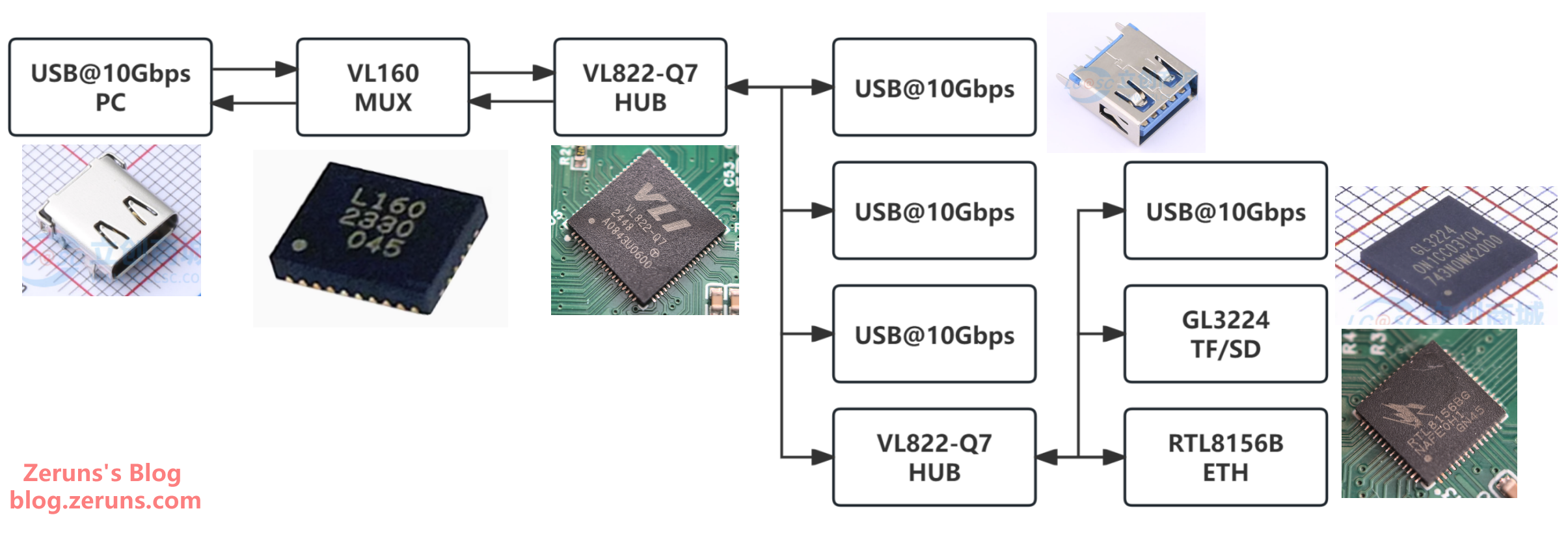
In this scenario, the USB data line first passes through the VL160 level-flip chip (enabling reversible Type-C insertion). The flipped USB signals are then sent to the VL822 hub chip, which splits one USB input into four USB outputs.
When connected to a 480 Mbps interface instead of 5 Gbps or higher, the USB signal bypasses the VL160 chip and goes directly into the VL822 hub, yielding a maximum downstream rate of 480 Mbps.
Expansion Dock Power Hardware Block Diagram:
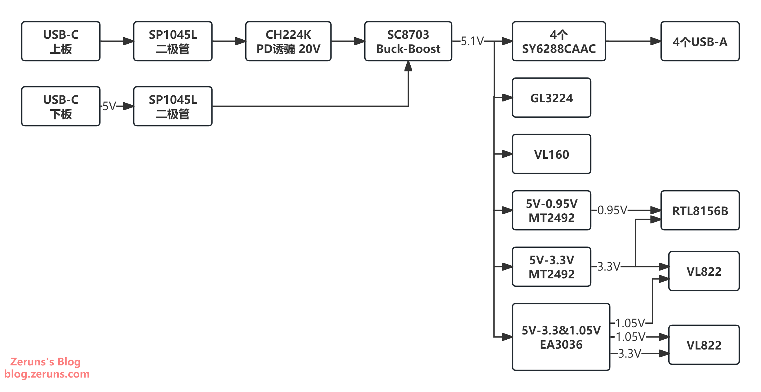
The SY6288CAAC is a power switch with built-in over-current protection. If the downstream load exceeds 2 A, the switch opens, cutting off power and pulling the OC pin low to alert the controller of the over-current condition.
Performance Tests
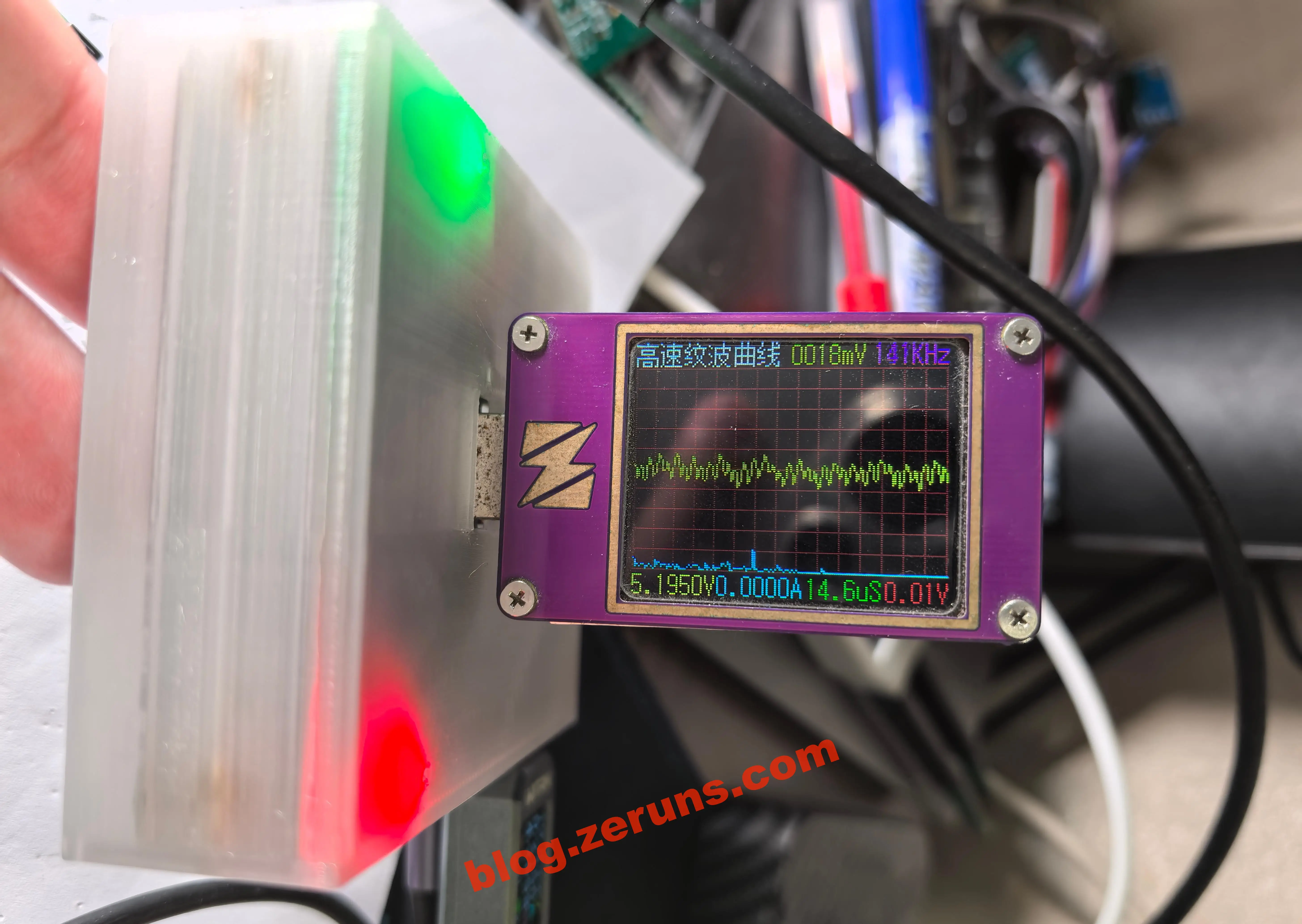
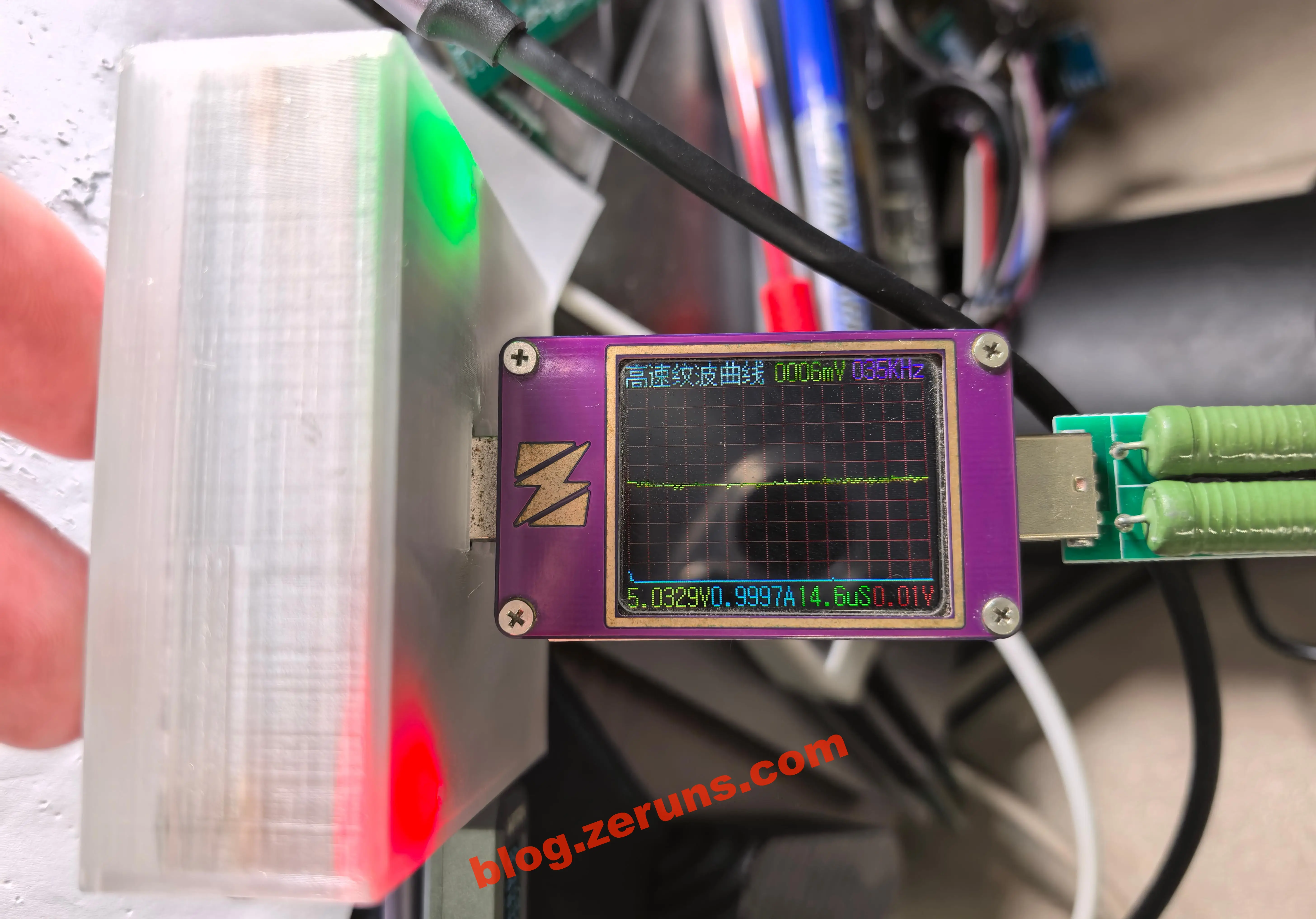
TYPE-A Port Output Ripple
No load: ~18 mV ripple
With 1 A load: ~6 mV ripple
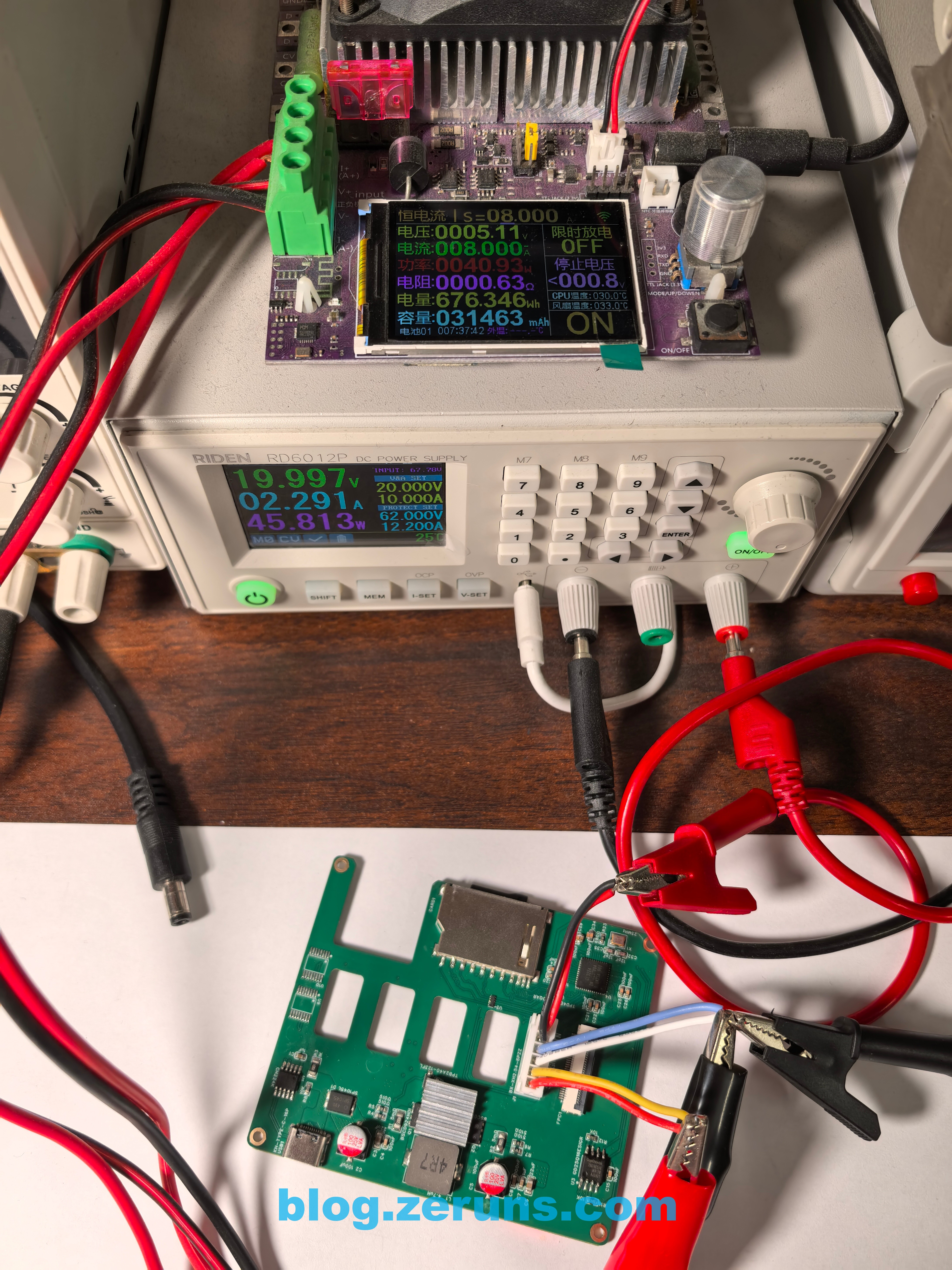
Power Conversion Efficiency
| Input Voltage (V) | Input Current (A) | Input Power (W) | Output Voltage (V) | Output Current (A) | Output Power (W) | Efficiency (%) |
|---|---|---|---|---|---|---|
| 19.997 | 2.291 | 45.81 | 5.11 | 8 | 40.88 | 89.23 |
| 19.998 | 1.122 | 22.44 | 5.15 | 3.999 | 20.59 | 91.79 |
| 19.998 | 0.569 | 11.38 | 5.18 | 2.002 | 10.37 | 91.14 |
| 4 | 2.839 | 11.36 | 5.20 | 2 | 10.40 | 91.58 |
| 4 | 8.063 | 32.25 | 5.17 | 5 | 25.85 | 80.15 |
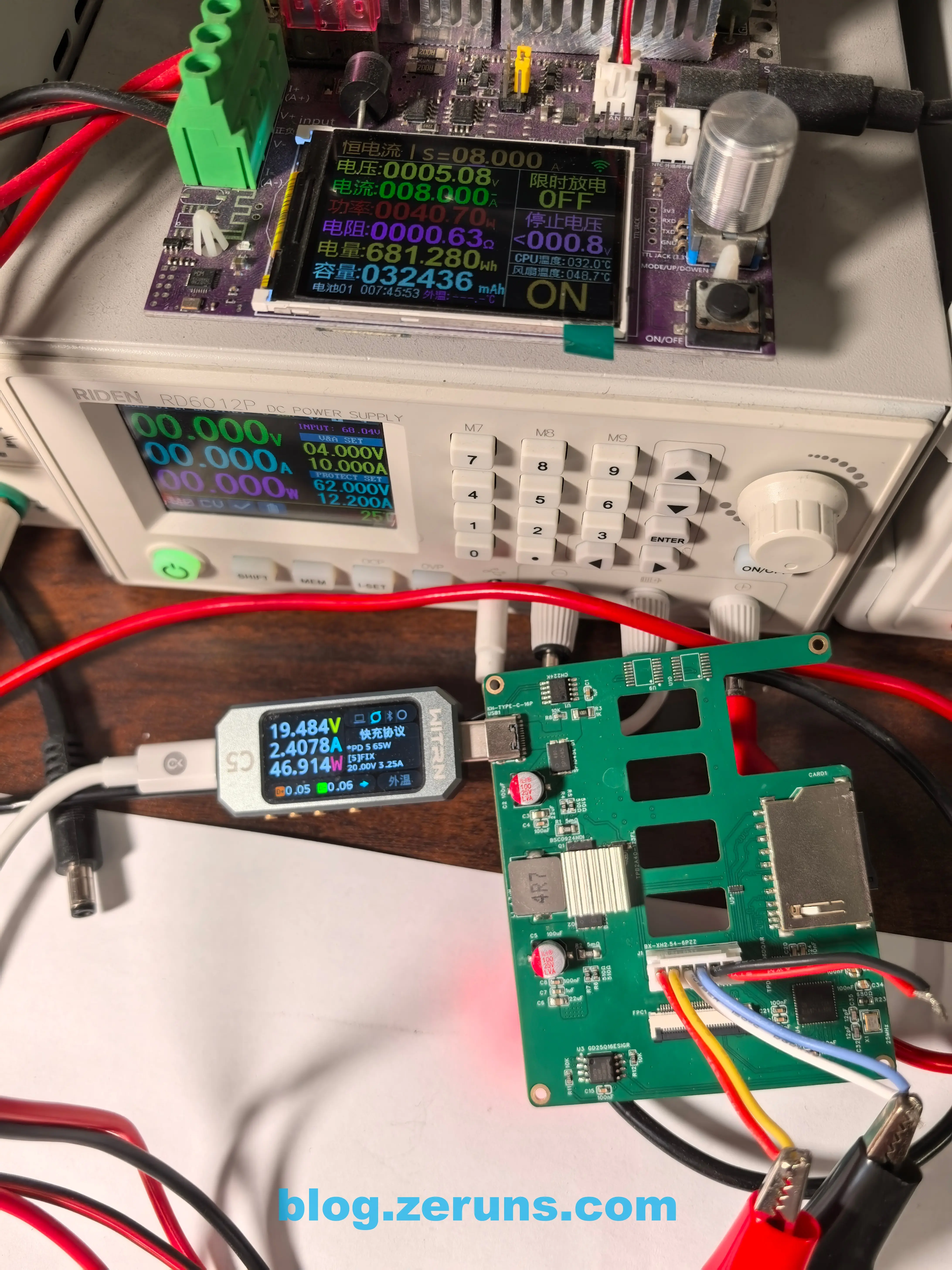
PD Fast-Charge Negotiation Test
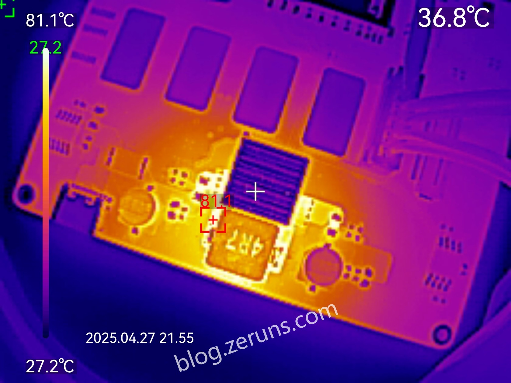
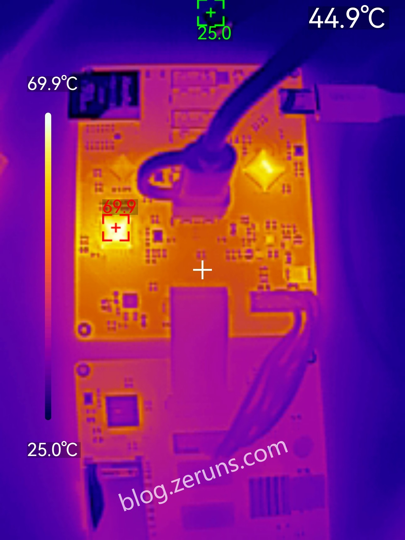
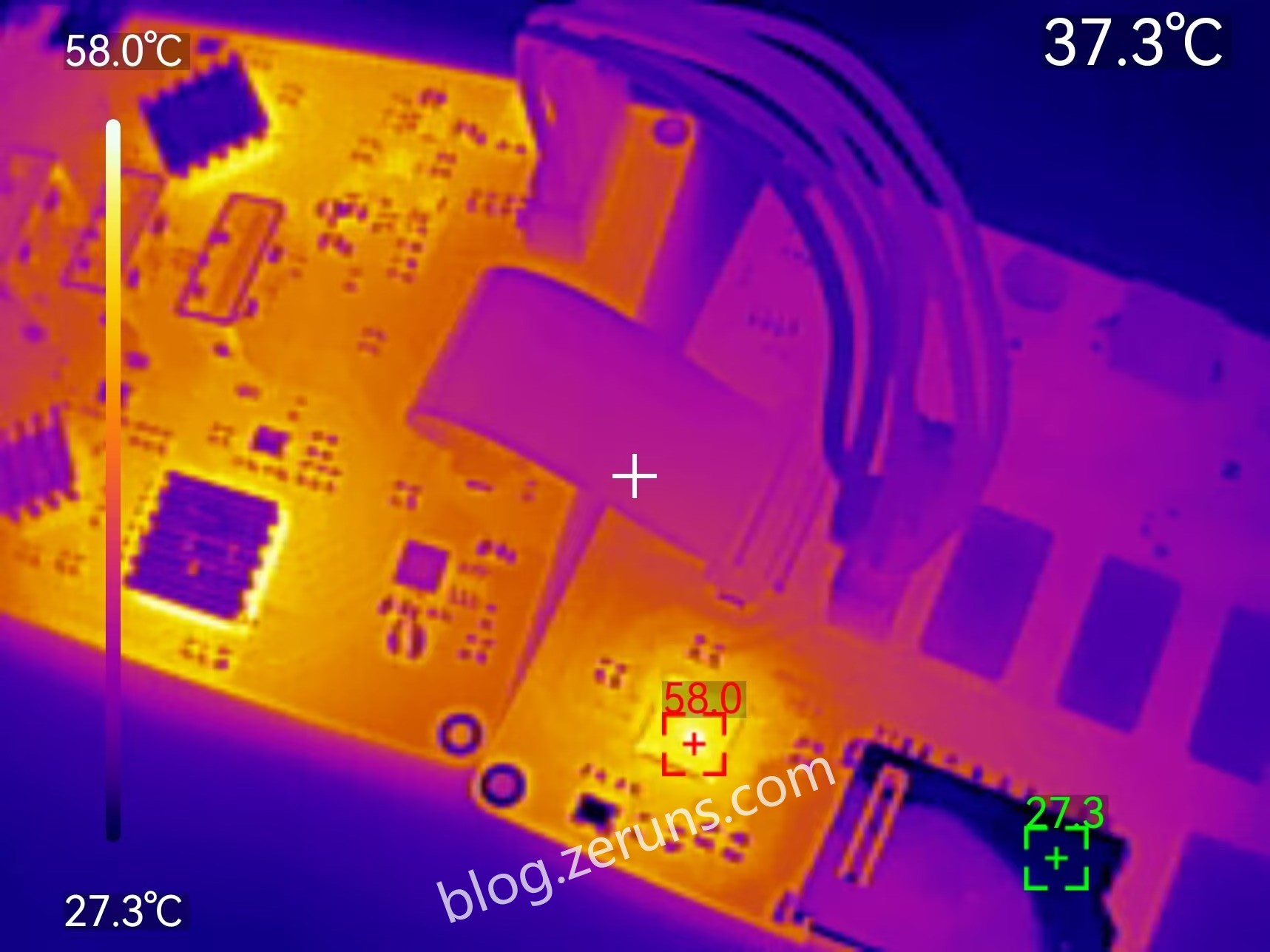
Thermal Imaging
MOSFET temperature ~81 °C when the 5 V power circuit delivers 8 A (ambient ~27 °C)
VL822 chip temperature ~70 °C under full read/write load (ambient ~25 °C)
GL3224 chip temperature ~58 °C under full read/write load (ambient ~27 °C)
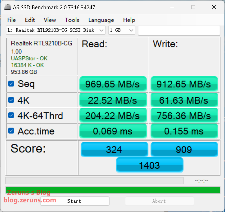
USB Throughput Test
The dock was connected to a computer's USB @ 10 Gbps port, then an HDD enclosure (RTL9210B) was attached. AS SSD Benchmark yielded: 969.65 MB/s read, 912.65 MB/s write.
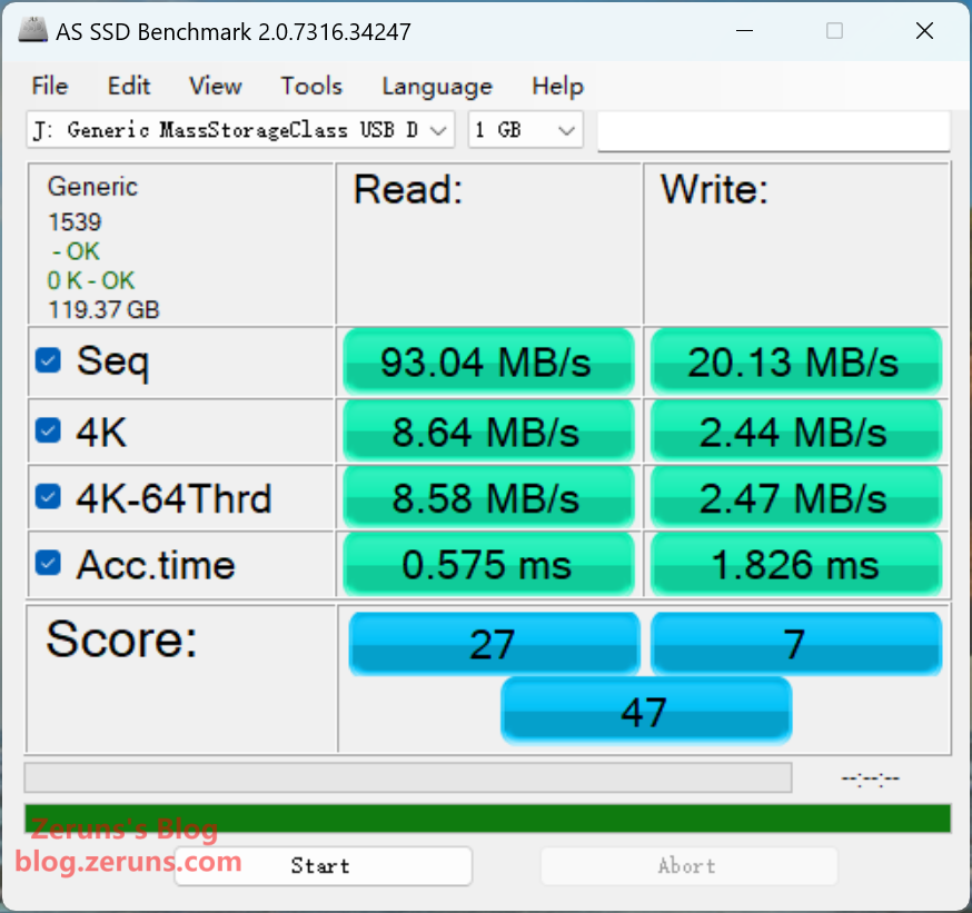
TF/SD Card Reader Speed Test
Tested with a Samsung EVO Plus TF card: 93.04 MB/s read, 20.13 MB/s write.
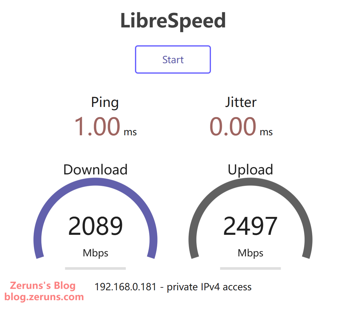
2.5 G Ethernet Speed Test
Using an internal speed-test server: 2089 Mbps download, 2497 Mbps upload.
Replication Notes
- The enclosure was 3D-printed; the 3D model files are available in the download links at the end of the article.
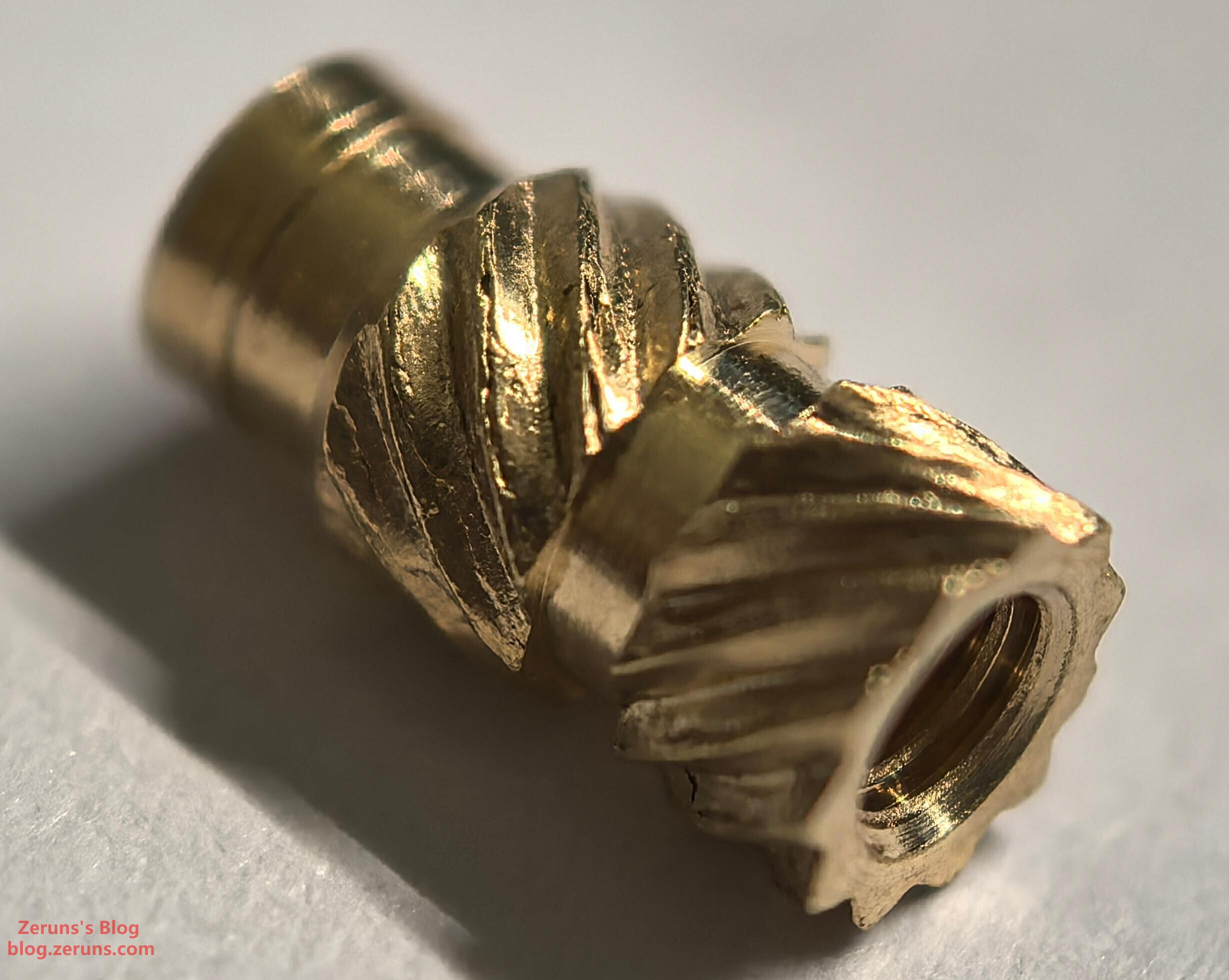
- The enclosure's screw holes require M2.5 heat-pressed nuts—heat them with a soldering iron and press them into place.
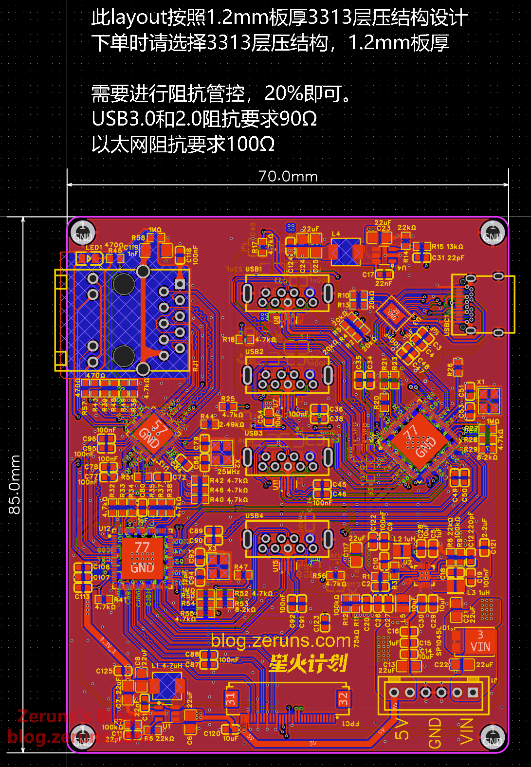
- When ordering the PCB, select the JLC04121H-3313 laminate structure with 1.2 mm board thickness, and be sure to perform impedance matching.
- Some systems may not reach full Ethernet speeds; you'll need to install the driver contained in the
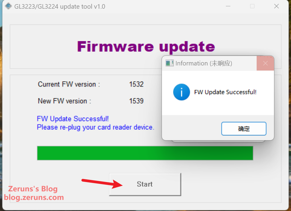
绿联USB有线网卡-RTL芯片-全系统_UGREEN_EthernetAdapter Driver_V1.01.ziparchive (see download links at the end). - Some systems may experience reduced card-reader performance; you can try upgrading the firmware using the tool in the
GL3224 update tool v1.0folder in the resources below. The factory firmware version is 1532, and the latest is 1539. If you don't need to upgrade, you can omit soldering the Flash chip. - Be sure to order the 30-pin FPC cable and the 6-pin XH2.54 cable in the reverse orientation.
M2.5 × 8 × 4 heat-pressed nuts
Schematics
Top Board
Bottom Board
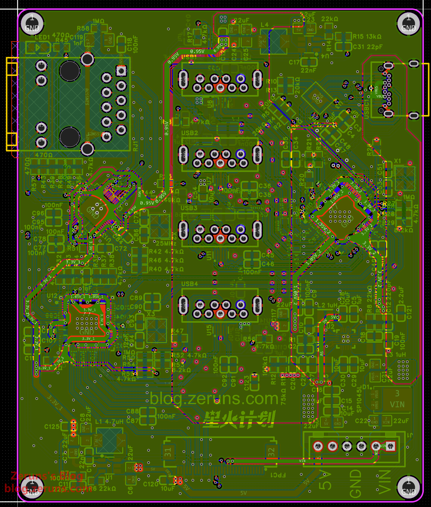
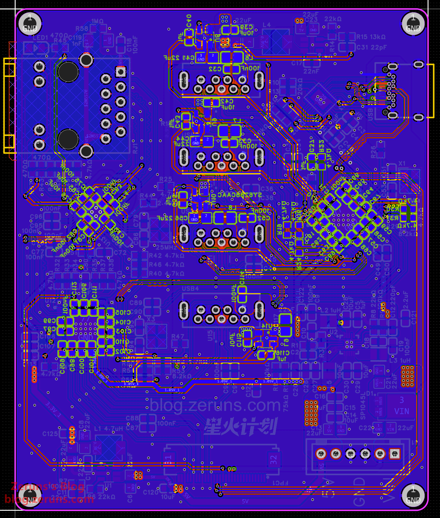
PCB Layouts
Top Board
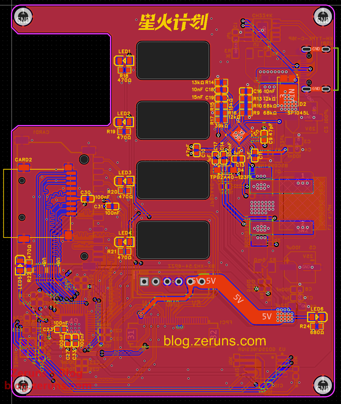
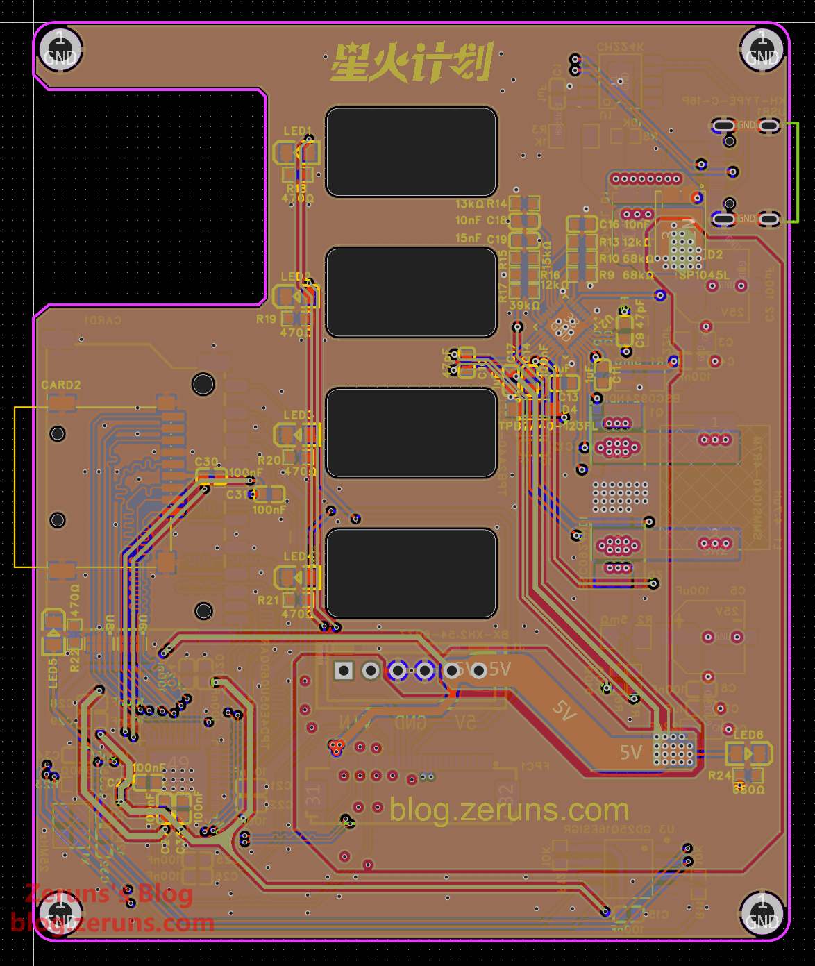
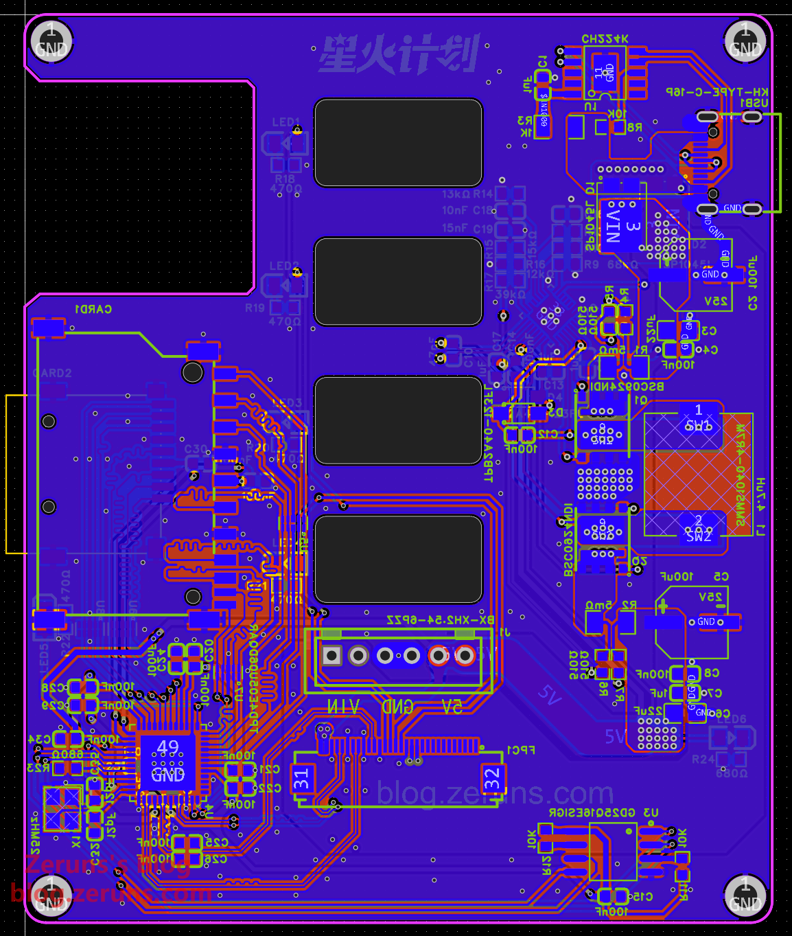
Bottom Board
Component Purchase Links
Most component purchase links for this project can be found here:
- 0603电阻电容样品本:https://s.click.taobao.com/ri755xr
- VL160芯片:https://s.click.taobao.com/xRw35xr
- VL822芯片:https://s.click.taobao.com/o5V35xr
- GL3224芯片:https://s.click.taobao.com/lj98olr
- SC8703QDER芯片:https://s.click.taobao.com/n8fz4xr
- RTL8156B芯片:https://s.click.taobao.com/dkC3olr
- TypeC母座24P:https://s.click.taobao.com/kWht4xr
- TypeC母座16P:https://s.click.taobao.com/SaRr4xr
It is recommended to purchase parts from the LCSC online store: https://activity.szlcsc.com/invite/D03E5B9CEAAE70A4.html
By clicking the BOM table in the LCSC open-source link, you can instantly import all required components into your LCSC shopping cart.
Resource Download Links
The following links include the LCSC EDA project, PDF schematics, PCB Gerber files, datasheets for all chips used, 3D enclosure model files, GL3224 firmware upgrade tool, and the RTL8156B driver.
Baidu Netdisk: https://pan.baidu.com/s/1uY0DD40T5NeZS1X4UwaPng?pwd=nvbx (Extraction code: nvbx)
123 Cloud Drive: https://www.123684.com/s/2Y9Djv-106vH?提取码:66SY
If you find this useful, feel free to show your appreciation by sending me a tip via the 123 Cloud Drive link above. If this appears as a WeChat article (public account: zeruns-gzh), you can also click the “Like Author” button below the article to support me. Thank you.
Other Open-Source Project Recommendations
- Published an open-source three-phase energy meter for easy home power monitoring: https://blog.zeruns.com/archives/771.html
- An LVGL project template based on STM32F407 (MSP3526 display), including FreeRTOS and bare-metal versions: https://blog.zeruns.com/archives/788.html
- Open-sourced an STM32-based synchronous-rectification Buck–Boost digital power supply: https://blog.zeruns.com/archives/791.html
- LM25118 auto boost/buck adjustable DCDC power module: https://blog.zeruns.com/archives/727.html
- Open-source EG1164 high-power synchronous-rectification boost module, up to 97% efficiency: https://blog.zeruns.com/archives/730.html
- 4G environmental-monitoring node based on Gizwits Air700E (temperature, humidity, pressure, etc.), uploading data to Alibaba Cloud IoT via MQTT: https://blog.zeruns.com/archives/747.html
- Open-sourced an intelligent electronic load based on CH32V307 (embedded competition entry): https://blog.zeruns.com/archives/785.html
- Open-source EG1151 high-power synchronous-rectification adjustable buck–boost power module (supports Type-C PD fast-charge input): https://blog.zeruns.com/archives/794.html
- Open-source 140 W + 65 W buck–boost PD 3.1 fast-charging module (2 C + 1 A ports), IP6557 + IP6538, for a 205 W desktop charger: https://blog.zeruns.com/archives/801.html
Recommended Reading
- Cost-effective and affordable VPS/cloud server recommendations: https://blog.zeruns.com/archives/383.html
- Minecraft server setup tutorial: https://blog.zeruns.com/tag/mc/
- A step-by-step 1Panel guide for one-click Halo blog deployment | Enterprise website/personal blog setup tutorial: https://blog.zeruns.com/archives/858.html
- Overview of 4 user-friendly control panels for one-click launches of various servers (Minecraft modpacks, Palworld, 7 Days to Die, CSGO, etc.): https://blog.zeruns.com/archives/808.html
- Quick unboxing review of the Ultra7-265K and GIGABYTE Z890M-AORUS-ELITE-WIFI7 motherboards: https://blog.zeruns.com/archives/863.html
- Flarum forum website setup tutorial—build a community forum from scratch: https://blog.zeruns.com/archives/866.html


Comment Section