


Operational Amplifier (Op-Amp) Beginner's Guide: From Theory to Practice
📑 Table of Contents
- What is an Operational Amplifier?
- Op-Amp Family Tree: More Than Just One Type
- Open-Loop Operation: When an Op-Amp Becomes a Comparator
- Introducing Negative Feedback: Taming the Wild Horse
- Voltage Follower: The Most Basic and Practical Circuit
- Non-Inverting Amplifier: Same Direction, Custom Amplification
- Inverting Amplifier: Signal Flipped 180°, Plus Amplification
- Virtual Short and Virtual Open: The Master Keys to Op-Amp Analysis
- ⚡ Common Beginner Pitfalls (Avoidance Guide)
- 🔍 Quick Selection Guide: Which Op-Amp for Which Scenario
- 📊 Key Parameters Explained
- 🔧 Hands-On Lab: Build Your First Op-Amp Circuit on a Breadboard
- Appendix: Classic Op-Amp Models Quick Reference
▶ Electronics/MCU Tech Exchange QQ Group: 2169025065
▶ eeClub - Electronics Engineer Community: https://bbs.eeclub.top/
1. What is an Operational Amplifier?
1.1 In a Nutshell
An Operational Amplifier (Op-Amp) is an integrated circuit device that can amplify a tiny voltage difference many times over. It is called an "operational" amplifier because, when it was first invented, it was used in analog computers to perform mathematical operations like addition, subtraction, multiplication, division, differentiation, and integration.
You can think of it as a voltage "lever": you apply a tiny force (voltage difference) on one end, and it outputs a multiplied force (output voltage) on the other. And this "lever ratio" can be customized by you through peripheral circuits—this is exactly where the magic of the op-amp lies.
1.2 A Brief History
In 1965, Fairchild Semiconductor introduced the world's first integrated op-amp chips, the μA702 and μA709, pioneering the era of op-amps transitioning from discrete components to integrated circuits. Later, in 1968, they released the legendary μA741—derivatives of this chip are still in production and use today. It can be considered the "workhorse" of the op-amp world: rugged, durable, and highly cost-effective.
Today, op-amps are everywhere—from the audio amplifier in your smartphone to industrial sensor signal conditioning, and electrocardiogram (ECG) detection in medical instruments.
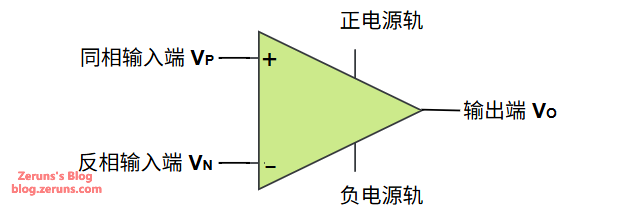
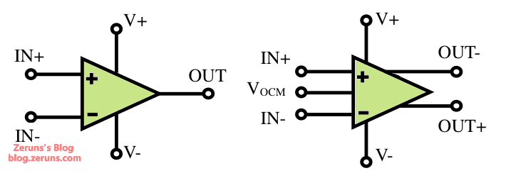
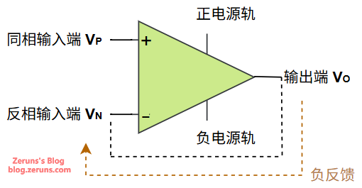
Figure 1: Standard Op-Amp Circuit Symbol. The
+terminal is the non-inverting input (the output is in phase with it), and the-terminal is the inverting input (the output is 180° out of phase with it). Two inputs, one output, plus positive and negative power supplies—these make up the complete "interface" of an op-amp.
2. Op-Amp Family Tree: More Than Just One Type
Many people think "an op-amp is just an op-amp" when they first start learning. However, after decades of development, op-amps have branched out into many specialized types. Understanding this family tree will help you make informed decisions during component selection.
| Type | Core Characteristics | Typical Applications |
|---|---|---|
| General Purpose (e.g., LM358, μA741) | Balanced performance, low cost | Teaching, low-frequency signal processing |
| Precision (e.g., OP07, OPA277) | Input offset voltage V_{OS} < 1\text{mV}, ultra-low temperature drift | Precision measurement, instrumentation front-end |
| Rail-to-Rail (RRIO) | Input/output voltages can swing very close to the power supply rails | Low-voltage battery-powered devices |
| High Speed | Extremely high Slew Rate (SR), wide bandwidth | High-speed ADC drivers, video signals |
| Low Noise (e.g., NE5532) | Extremely low noise density | Audio preamplifiers, Hi-Fi equipment |
| Instrumentation Amp (e.g., AD620) | Extremely high CMRR, ultra-high input impedance | Bridge sensors, ECG monitors |
| Current Sense Amp | Can operate at common-mode voltages much higher than its own supply | Battery charge/discharge monitoring, motor current sampling |
| Transimpedance Amp (TIA) | Converts current input to voltage output | Photodiode amplification |
| Differential Amp | Amplifies the difference between two inputs, rejects common-mode | Differential signal transmission |
| Isolation Amp | Capacitive/inductive/optical isolation between input and output | Medical devices, high-voltage safety scenarios |
| Programmable Gain Amp (PGA) | Gain is adjustable via digital signals | Auto-ranging systems |
Memory Trick for Beginners: Don't rote memorize. Usually, when starting a project, ask yourself three questions: Is the signal frequency high? Are the precision requirements strict? Is the power supply voltage low? These three questions will generally help you narrow down the candidates.
3. Open-Loop Operation: When an Op-Amp Becomes a Comparator
3.1 Open-Loop Gain: The Op-Amp's "Raw Power"
An op-amp is born with a superpower: Open-Loop Gain (A_{OL}). What does "open-loop" mean? It means there is no connection between the output and input terminals—no feedback network, just the bare op-amp.
In this state, the op-amp's behavior can be described by a simple formula:
Where:
- V_P: Voltage at the non-inverting input
- V_N: Voltage at the inverting input
- A_{OL}: Open-loop gain (typically 100,000 times or higher, i.e., 100 dB)
- V_O: Output voltage
What does this mean? Even if there's only a tiny 1 mV difference between the two inputs, after being amplified 100,000 times, the theoretical output should be 100 V. But reality dictates that you can't output 100 V because the op-amp's output is capped by its power supply voltage.
3.2 Power Supply Rails: The "Ceiling" and "Floor"
An op-amp needs power to work. There are two common ways to supply power:
- Dual Supply: For example, \pm 12\text{V}. The op-amp's output can swing above and below ground (0V), producing both positive and negative voltages.
- Single Supply: For example, +12\text{V} and GND. The op-amp's output can only swing between 0V and +12\text{V}.
The upper and lower limits of the op-amp's supply voltage are called Power Supply Rails. The output voltage can never exceed the rails—just like you can't jump through the ceiling, no matter how high you jump.
Analogy: Open-loop gain is like a person who can lift 1,000 times their own body weight, but there is a ceiling and a floor limiting their range of motion. No matter how strong they are, the highest and lowest points their hands can reach are determined by the ceiling and the floor. This "ceiling" is the positive supply rail, and the "floor" is the negative supply rail (or ground).
3.3 Comparator Mode: It's Either 0 or 1
By combining the open-loop gain formula with the supply rail clipping effect, we get the simplest operating mode of an op-amp—a Comparator:
| Condition | Output Result |
|---|---|
| V_P > V_N (Non-inverting voltage is higher) | V_O ≈ Positive supply rail limit |
| V_P < V_N (Inverting voltage is higher) | V_O ≈ Negative supply rail limit |
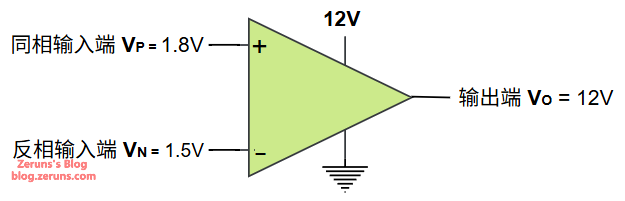
Figure 2: When V_P = 1.8\text{V}, V_N = 1.5\text{V}, V_P - V_N = +0.3\text{V} > 0, the op-amp output is "pushed" to the positive supply rail (+12\text{V} in this example).
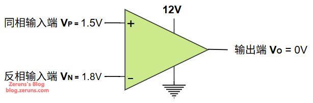
Figure 3: When V_P = 1.5\text{V}, V_N = 1.8\text{V}, V_P - V_N = -0.3\text{V} < 0, the op-amp output is "pulled" to the negative supply rail (0\text{V} in this example, single supply).
In other words, an op-amp in an open-loop state acts like a binary referee—it only judges which of the two inputs is larger and outputs an extreme result. This application is very similar to a dedicated comparator chip.
❗ Pro Tip: Although a general-purpose op-amp can be used as a comparator, it is not recommended for high-speed or precision comparison scenarios. There are three reasons:
(1) Op-amps take time to recover from saturation, which is much slower than dedicated comparators.
(2) Op-amps usually lack internal hysteresis, making the output prone to chatter/jitter from input noise.
(3) Some op-amps may experience "phase reversal" when deeply saturated. If you really need to compare two signals, using a dedicated comparator chip (like the LM393) is much safer.
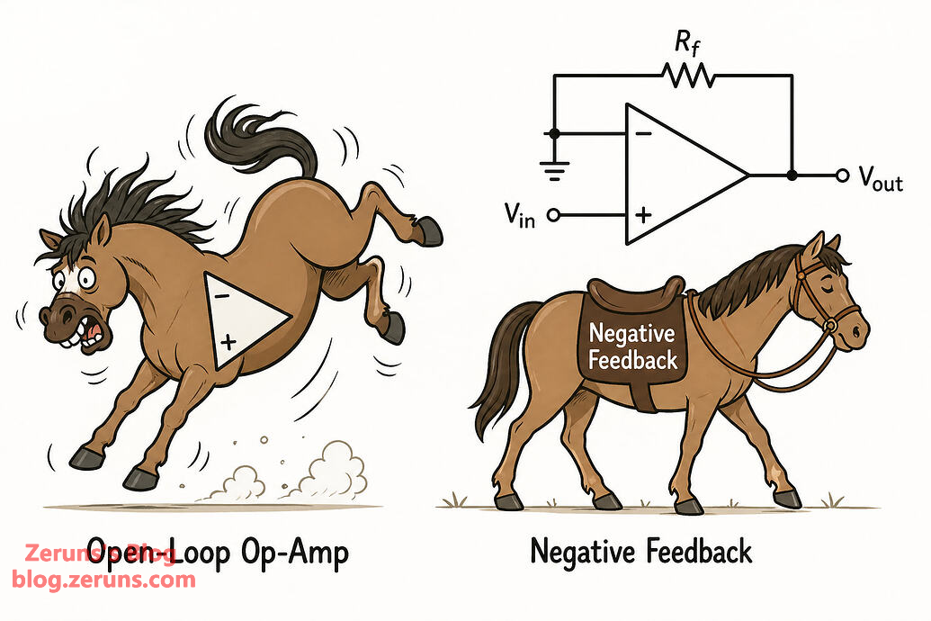
4. Introducing Negative Feedback: Taming the Wild Horse
An open-loop op-amp is too "wild"—its massive gain prevents it from doing delicate linear amplification; the slightest breeze at the input will crash the output straight into the supply rail. To make this "wild horse" docile and usable, we need a trick: Negative Feedback.
4.1 What is Negative Feedback?
Imagine you are adjusting your shower water temperature. You put your hand under the water (sensing the temperature). If it's too hot, you turn down the hot water (reducing output); if it's too cold, you turn up the hot water (increasing output). You continuously detect, compare, and adjust until the water stabilizes at your desired temperature. This process is negative feedback—feeding a portion of the output signal back to the input to counteract deviations.
In op-amp circuits, negative feedback means connecting the output terminal V_O back to the inverting input terminal V_N using components like resistors. Consequently:
- If V_O goes slightly "higher" than expected → The voltage fed back to V_N also increases → V_P - V_N decreases → The op-amp reduces its output.
- If V_O goes slightly "lower" than expected → The voltage fed back to V_N also decreases → V_P - V_N increases → The op-amp increases its output.
This closed-loop automatic adjustment process happens incredibly fast (usually in microseconds), ultimately stabilizing the output at a precise value.
Analogy: An open-loop op-amp is like a race car with the gas pedal stuck to the floor—it can only go top speed or completely stop. Adding negative feedback is like installing cruise control—you set a target speed (V_P), and the system automatically tweaks the throttle (V_O) so the actual speed precisely matches your setting.
5. Voltage Follower: The Most Basic and Practical Circuit
5.1 Circuit Structure
If you connect the op-amp's output V_O directly with a wire back to the inverting input V_N, you get a Voltage Follower:
Looking at the schematic might confuse you: Output connected straight back to the input? What's the point? Doesn't the output just equal the input?
Exactly! That is precisely its value. A voltage follower's output voltage equals its input voltage (Gain = 1), but it has extremely high input impedance and extremely low output impedance. In plain English: It draws virtually no current from the signal source but can supply a substantial amount of current to the subsequent load circuit.
5.2 Real-Life Analogy
Imagine you need to trace a masterpiece painting. You can't put your hand directly on the original (it would damage it), and you dare not press hard (requires high input impedance). But you want an exact duplicate on another piece of paper (Output = Input), and you want to be able to press hard on this duplicate without affecting the original (strong output driving capability).
A voltage follower acts as this Buffer—it builds an "isolation wall" between the signal source and the load, making the source feel like there's nothing pulling on it (high input impedance), while giving the load a robust, strong driving signal (low output impedance).
5.3 When to Use a Voltage Follower?
- A sensor (like a temperature probe or a photoresistor divider) has high output impedance and cannot directly drive an ADC. Place a voltage follower in between.
- Multiple sub-circuits need to share the same reference voltage without interfering with each other. Place a follower in front of each branch.
- When transmitting a signal over a long distance, use a follower at the receiving end for impedance matching.
❗ Pro Tip: There's a common beginner mistake when building a voltage follower—forgetting to power the op-amp! Yes, many people draw schematics assuming power is implied, but forget to wire the supply pins during actual soldering. Also, while seemingly simple, if the op-amp lacks sufficient bandwidth, the output won't keep up with rapidly changing input signals, causing noticeable delay and distortion. So, when tracking high-frequency signals, remember to check the op-amp's Unity Gain Bandwidth (UGBW).
6. Non-Inverting Amplifier: Same Direction, Custom Amplification
6.1 Circuit Structure
The wiring for a Non-Inverting Amplifier is as follows: The input signal enters the non-inverting terminal, and a feedback network (two resistors, R_1 and R_2) is connected between the inverting terminal and the output:
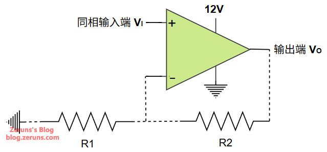
- R_1: From the inverting terminal to ground (Gain resistor R_G)
- R_2: From the output terminal to the inverting terminal (Feedback resistor R_F)
6.2 How Deep Negative Feedback "Auto-Adjusts"
Let's walk through how the circuit works step-by-step. Assume initially V_I = 1\text{V} and R_1 = R_2 = 1\text{k}\Omega:
- V_P = V_I = 1\text{V} (Input signal directly applied to the non-inverting terminal)
- The instant power is applied, V_O might be 0\text{V}, so after passing through the voltage divider of R_2 and R_1, V_N \approx 0\text{V}
- Thus, V_P - V_N = 1\text{V} - 0\text{V} = +1\text{V} > 0. The op-amp starts "pushing" the output hard.
- V_O steadily rises, and V_N = V_O \times \frac{R_1}{R_1 + R_2} rises with it.
- When V_O reaches 2\text{V}, V_N = 2\text{V} \times \frac{1\text{k}}{1\text{k}+1\text{k}} = 1\text{V} = V_P
- At this point, V_P - V_N = 0. The op-amp stops changing, and V_O stabilizes at 2\text{V}.
Final result: Input 1V, Output 2V. Amplified 2 times!
6.3 Mathematical Derivation (Let's walk through it)
Using two key properties of op-amps:
- Virtual Short (Under deep negative feedback, V_P = V_N): So, V_N = V_P = V_I
- Virtual Open (Input terminals draw almost no current): The current flowing through R_1 equals the current flowing through R_2.
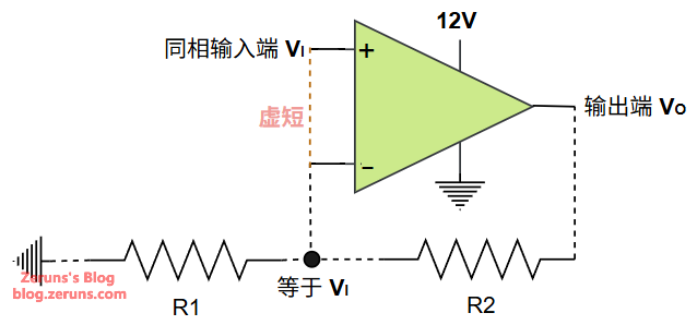
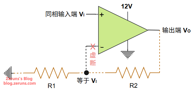
According to Ohm's Law (I = \frac{U}{R}), the current through R_1 is:
The current through R_2 is:
Since the two currents are equal:
Rearranging gives:
Core Formula — Non-Inverting Amplifier Gain:
A_V = 1 + \frac{R_2}{R_1}
6.4 Simulation Verification
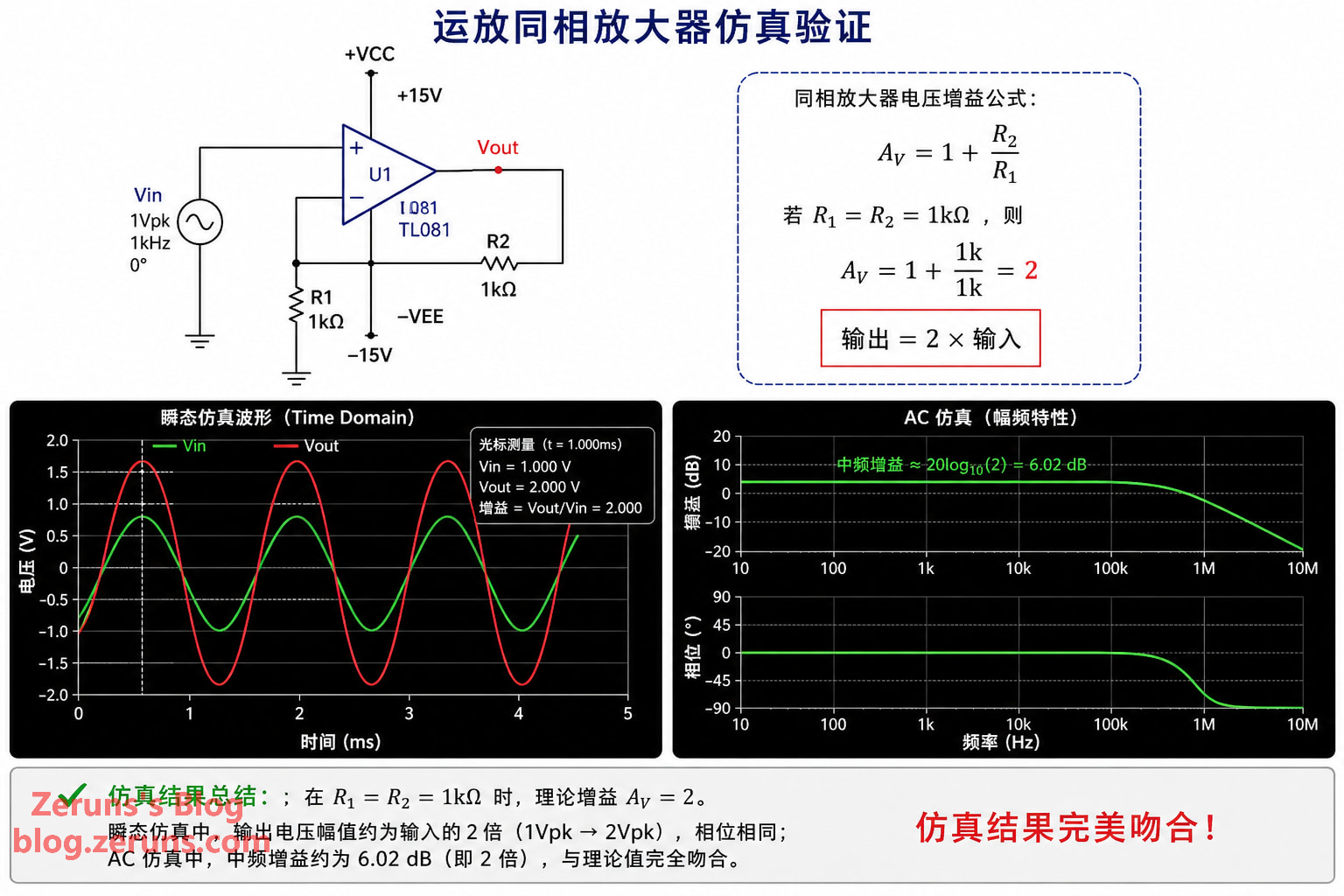
If R_1 = R_2 = 1\text{k}\Omega, then A_V = 1 + \frac{1\text{k}}{1\text{k}} = 2. Output = 2 \times Input. The simulation perfectly matches.
Note: The gain formula can give arbitrarily large multipliers on paper, but the actual output voltage is still limited by the supply rails. For instance, if powered by \pm 5\text{V} with a 2\text{V} input, setting a gain of 10 will still clip the output at roughly +5\text{V} (saturation).
6.5 Summary of Non-Inverting Amplifier Features
| Feature | Description |
|---|---|
| Gain Formula | A_V = 1 + R_2 / R_1 |
| Gain Range | ≥ 1 (Cannot be less than 1) |
| Input Impedance | Extremely High (Input signal is connected to the non-inverting pin; op-amp input impedance is usually in the MΩ range) |
| Output/Input Phase | In-Phase (0° phase shift) |
❗ Pro Tip:
- Resistor Selection: R_1 and R_2 shouldn't be too large (to avoid high thermal noise) nor too small (to avoid high power consumption and heavy load on the op-amp output). A common range is 1\text{k}\Omega \sim 100\text{k}\Omega.
- Bias Current Effect: If the op-amp's input bias current I_B is relatively large (like in bipolar op-amps), it creates a small voltage drop across the parallel combination of R_1 and R_2 (R_1 // R_2), and this drop will be amplified. For high-precision applications, it's recommended to add a resistor equal to R_1 // R_2 between the non-inverting terminal and ground to cancel out the error caused by the bias current.
- PCB Layout: The feedback resistor R_2 should be placed as close to the op-amp's inverting input pin as possible to reduce parasitic capacitance and EMI.
7. Inverting Amplifier: Signal Flipped 180°, Plus Amplification
7.1 Circuit Structure
The wiring for an Inverting Amplifier is as follows: The input signal connects to the inverting terminal via resistor R_1, the non-inverting terminal is tied directly to ground, and feedback resistor R_2 bridges the output and the inverting terminal:
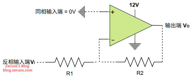
7.2 How Does the Circuit Work?
- The non-inverting terminal is grounded, so V_P = 0\text{V}.
- By the "Virtual Short" rule, V_N = V_P = 0\text{V} (The inverting terminal is "forced" to 0V — this is the famous Virtual Ground concept).
- The input signal V_I is applied to the left of R_1. The right of R_1 (which is V_N) is 0V, so the current through R_1 is I = V_I / R_1.
- By the "Virtual Open" rule, this current cannot flow into the op-amp input, so it must entirely flow through R_2.
- The current through R_2 is I = (0 - V_O) / R_2 = -V_O / R_2.
- Equating the two currents: V_I / R_1 = -V_O / R_2.
- Thus, V_O = -V_I \times \frac{R_2}{R_1}.
What does the negative sign mean? It means the output is out-of-phase with the input (shifted by 180°)!
7.3 Mathematical Derivation
Core Formula — Inverting Amplifier Gain:
A_V = -\frac{R_2}{R_1}
Note that the gain of an inverting amplifier can be less than 1 (an attenuator), whereas the minimum gain for a non-inverting amplifier is 1.
7.4 Simulation Verification
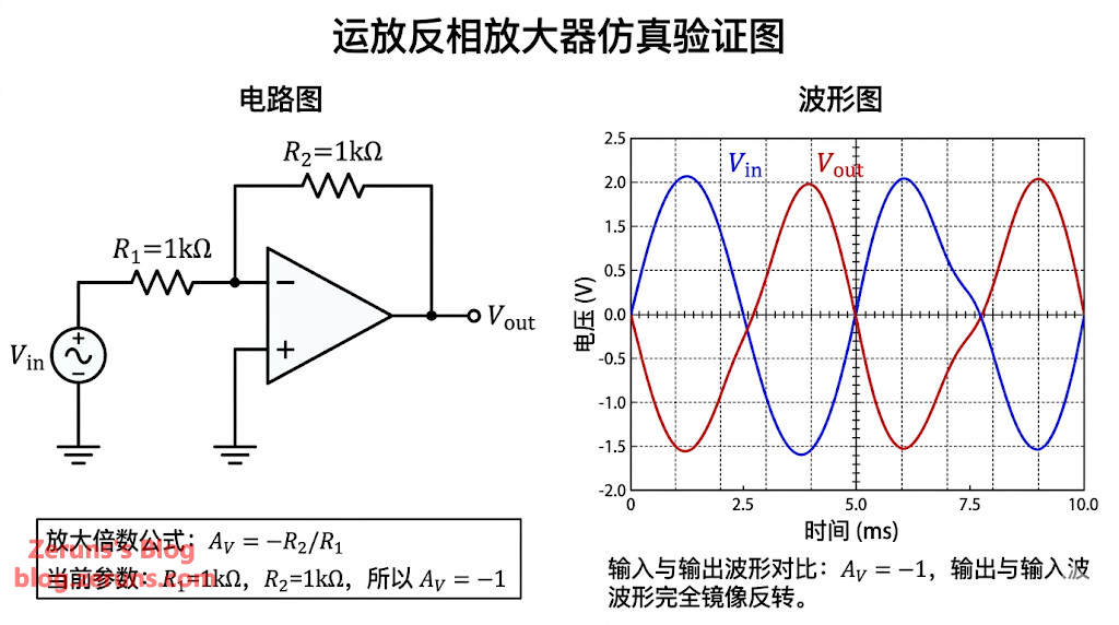
If R_1 = R_2 = 1\text{k}\Omega, then A_V = -1. The output waveform is a perfect mirror inversion of the input.
7.5 Summary of Inverting Amplifier Features
| Feature | Description |
|---|---|
| Gain Formula | A_V = -R_2 / R_1 |
| Gain Range | Can be < 1 (Attenuate) or > 1 (Amplify) |
| Input Impedance | R_{in} \approx R_1 (Relatively low! This is a crucial distinction) |
| Output/Input Phase | Inverted (180° phase shift) |
7.6 Non-Inverting vs. Inverting: Which to Choose?
| Comparison | Non-Inverting Amplifier | Inverting Amplifier |
|---|---|---|
| Input Impedance | Extremely High (MΩ range) | Approximately R_1 (Usually kΩ range) |
| Gain Range | \ge 1 | Any (can attenuate) |
| Phase | 0° | 180° |
| Common-Mode Voltage | Input terminal sustains common-mode voltage | Input terminal common-mode voltage ≈ 0V (Virtual Ground) |
| Best Application | High-impedance signal sources (sensors) | Low-impedance sources, when phase inversion is needed |
❗ Pro Tip:
- Does an inverting amp need dual power supplies? Not necessarily. If your input signal is always positive (like a 0~2V sine wave), you can use a single supply, but you'll need to tie the non-inverting terminal to a mid-point reference voltage (like V_{CC}/2) instead of ground—this is called "biasing." If your input swings positive and negative, you must use a dual supply, or else the portion of the output below 0V will be clipped.
- The Input Impedance Issue: The input impedance of an inverting amplifier equals R_1. If you set R_1 to 1\text{k}\Omega, the signal source "sees" a 1\text{k}\Omega load. If the source has poor driving capability (high output impedance), the signal will be attenuated by voltage division, causing measurement errors.
- The Magic of Virtual Ground: Because the V_N node of an inverting amp is always 0V (virtual ground), it serves as the foundational topology for building Summing Amplifiers and Current-to-Voltage Converters (TIA).
8. Virtual Short and Virtual Open: The Master Keys to Op-Amp Analysis
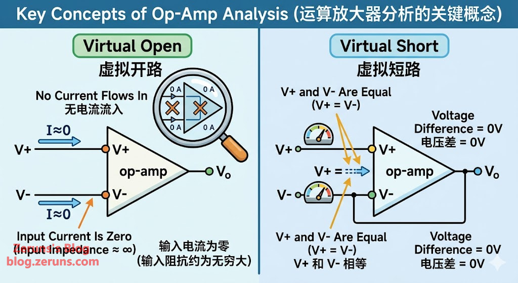
Anyone learning op-amps will inevitably encounter two concepts: Virtual Short and Virtual Open. These are the universal master keys for analyzing any linear op-amp circuit. But many tutorials just tell you to "memorize them". Here, we'll explain their true nature using practical analogies.
8.1 Virtual Open
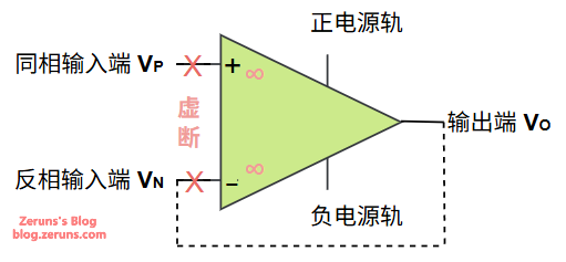
Definition: An op-amp's input terminals are designed to have extremely high input impedance (ideally infinite), meaning virtually no current flows in or out of them. It acts as if the internal connection is physically broken—but it's not actually broken, hence a "virtual" open.
Analogy: Imagine standing in front of a very high-impedance electrostatic voltmeter. The probe can sense your static voltage, but it pulls absolutely no charge from you—you don't even feel it's there. The op-amp's inputs act exactly like this "high-impedance voltage sensor."
Key Formula: I_P \approx 0, I_N \approx 0
8.2 Virtual Short
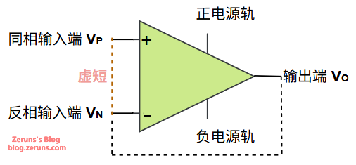
Definition: When an op-amp is operating with deep negative feedback, the non-inverting voltage V_P and the inverting voltage V_N become nearly identical. It acts as if the two terminals are shorted together—but again, they aren't physically shorted, hence a "virtual" short.
Why does a virtual short occur?
This is a direct result of the negative feedback mechanism. Remember the cruise control analogy from Chapter 4:
- The op-amp frantically adjusts V_O until V_P - V_N \approx 0.
- If V_P - V_N doesn't hit zero, the op-amp will keep "pushing" or "pulling" the output.
- Equilibrium is reached only when V_P \approx V_N.
Therefore, a virtual short is not an inherent property of the circuit; it is a forced outcome driven by negative feedback. If you remove the feedback loop (open-loop), the virtual short instantly disappears—V_P and V_N can have massive differences.
Key Formula: V_P \approx V_N (Strictly valid only under deep negative feedback)
8.3 Virtual Short + Virtual Open = Ultimate Analysis Tool
By combining these two concepts, analyzing almost any linear op-amp circuit degrades into middle-school math:
- Virtual Short tells you V_P = V_N, giving you the voltage of a crucial node.
- Virtual Open tells you the inputs draw no current, so you can analyze the current flowing through peripheral resistors as simple series loops.
- The rest is just writing out a few Ohm's Law equations and solving them.
8.4 Common Pitfalls for Beginners
- Assuming "Virtual Short" is unconditional. Virtual Short only holds under deep negative feedback AND within the linear operating region. When the op-amp is saturated (output hitting the supply rail), the virtual short vanishes.
- Assuming "Virtual Open" means you shouldn't connect anything to the inputs. Virtual Open simply implies almost zero current; however, voltage signals can still be "sensed". You can (and must) connect circuitry to the inputs.
9. ⚡ Common Beginner Pitfalls (Avoidance Guide)
Pitfall 1: Ignoring Supply Rails and Thinking the Gain Formula is Omnipotent
"I set the gain to 100, and inputted 0.5V. Why isn't the output 50V?"
Because your power supply is only 5V! The gain formula provides a theoretical value in the linear region, but the output voltage is permanently constrained by the "ceiling" of your power supply rails. The gain formula is the "wish"; the supply rail is the "reality".
Pitfall 2: Using Any Op-Amp as a Comparator Arbitrarily
General-purpose op-amps can act as makeshift comparators, but they are slow, lack hysteresis, and may suffer phase reversal. For precision comparison, always use a dedicated comparator.
Pitfall 3: Using an Inverting Amp with a Single Supply Without "Biasing"
The non-inverting pin of an inverting amplifier is typically tied to ground (0V), causing the output to swing around 0V. If you only have a single supply (e.g., 0~5V), the negative half-cycle will be clipped off entirely. The fix is to tie the non-inverting pin to a reference voltage of V_{CC}/2.
Pitfall 4: Extreme Resistor Values
- Too small (e.g., 10\Omega) → Excessive current; the op-amp can't drive the load, and the resistors overheat.
- Too large (e.g., 10\text{M}\Omega) → Severe thermal noise, and bias current creates significant errors.
Recommended range: 1\text{k}\Omega \sim 100\text{k}\Omega.
Pitfall 5: Ignoring Bandwidth Limits
Gain-Bandwidth Product (GBW) is constant. If you set the gain to 100, your bandwidth will only be GBW/100. Want to amplify a 100kHz signal by 100 times? You need an op-amp with a GBW \ge 10MHz.
Pitfall 6: Forgetting Decoupling Capacitors
You must place a 0.1\mu\text{F} ceramic capacitor (decoupling capacitor) as close as possible to the op-amp's power supply pins. Otherwise, the op-amp may self-oscillate—producing high-frequency noise at the output that wasn't in your input.
Pitfall 7: Exceeding Common-Mode Input Range
Many op-amps have a common-mode input range narrower than their supply rails (non-RRIO op-amps). If your input voltage exceeds this range, the op-amp might behave erratically or even suffer phase reversal.
10. 🔍 Quick Selection Guide: Which Op-Amp for Which Scenario
10.1 Selection Decision Tree
Start Selection
│
├─ Signal Frequency > 1MHz?
│ ├─ Yes → High-Speed Op-Amp (SR > 50V/µs, GBW > 50MHz)
│ └─ No → Continue
│
├─ Strict Precision Requirements? (Error < 0.1%?)
│ ├─ Yes → Precision Op-Amp (V_OS < 100µV, Drift < 1µV/°C)
│ └─ No → Continue
│
├─ Low Supply Voltage? (< 5V?)
│ ├─ Yes → Rail-to-Rail Op-Amp (RRIO)
│ └─ No → Continue
│
├─ High Signal Source Impedance? (> 100kΩ?)
│ ├─ Yes → FET/CMOS Input Op-Amp (I_B < 10pA)
│ └─ No → Continue
│
├─ Sensitive to Noise? (Audio/Precision Measurement?)
│ ├─ Yes → Low-Noise Op-Amp (Noise Density < 10nV/√Hz)
│ └─ No → Continue
│
├─ Need to Measure Current?
│ ├─ Yes → Current Sense Amplifier
│ └─ No → Continue
│
└─ No special requirements → General Purpose Op-Amp (LM358/LM324/TL074)
`
10.2 Scenario Quick Reference Table
| Application Scenario | Recommended Op-Amp Type | Key Parameters to Focus On | Example Models |
|---|---|---|---|
| Battery-Powered Portables | Low Power + RRIO | Quiescent Current < 1mA, RRIO | MCP6002, TLV9002 |
| Audio Preamplifier | Low Noise + Low Distortion | Noise Density < 5nV/√Hz, THD+N < 0.001% | NE5532, OPA1612 |
| Temp/Pressure Sensors | Precision + Low Drift | V_{OS} < 100\mu\text{V}, Drift < 1µV/°C | OP07, OPA277 |
| High-Speed ADC Driver | High Speed + Wide Bandwidth | SR > 50V/µs, Settling Time < 100ns | AD8051, THS4031 |
| Motor Current Sampling | Current Sense Amplifier | Common-Mode Range > 30V, CMRR > 100dB | INA181, MAX4080 |
| Photodiode Amplification | Transimpedance Amp (TIA) | Ultra-low I_B (< 1pA), Low Noise | OPA656, ADA4530-1 |
| ECG/EEG Measurement | Instrumentation Amplifier | CMRR > 100dB, Ultra-low Noise | AD620, INA128 |
| General Teaching/Low-Freq | General Purpose Op-Amp | Cheap, Accessible, Rugged | LM358 (Dual), TL074 (Quad) |
11. 📊 Key Parameters Explained
11.1 Static Parameters (DC Characteristics)
These parameters impact an op-amp's precision under direct current and low frequencies.
| Parameter | English Name | Function & Plain Explanation | Trend | Typical Value (General) | Typical Value (Precision) |
|---|---|---|---|---|---|
| Input Offset Voltage V_{OS} | Offset Voltage | "Inherent error" caused by transistor asymmetry inside the op-amp. Think of it as: Even if both inputs are exactly equal, the op-amp "thinks" they differ by V_{OS}. | ↓ Lower is better | 1~10 mV | < 100 µV |
| Offset Voltage Drift \frac{dV_{OS}}{dT} | Offset Voltage Drift | How much V_{OS} drifts for every 1°C temp change. For precision circuits, this is worse than initial V_{OS}—you can calibrate out static error, but drift is hard to compensate. | ↓ Lower is better | 5~20 µV/°C | < 1 µV/°C |
| Input Bias Current I_B | Input Bias Current | A tiny "maintenance current" required by the op-amp's inputs, originating from internal transistor bases/gates. | ↓ Lower is better | Bipolar: 10~200 nA; CMOS: < 1 pA | CMOS: < 10 pA |
| Input Offset Current I_{OS} | Input Offset Current | The difference between the I_B of the two inputs. I_B can be canceled with a balancing resistor, but the error from I_{OS} is tough to eliminate. | ↓ Lower is better | 5%~20% of I_B | 5%~20% of I_B |
| Input Voltage Range | Input Voltage Range | The max input voltage range the op-amp handles normally. Rail-to-Rail Input (RRI) covers the entire supply range; non-RRI is narrower (usually clipped by 1~2V). | ↑ Higher is better | V_{SS}+1.5\text{V} \sim V_{DD}-1.5\text{V} (Non-RRI) | V_{SS} \sim V_{DD} (RRI) |
| Output Voltage Swing | Output Voltage Swing | The max voltage range the op-amp can actually output. Similar to input range, separated into Rail-to-Rail Output (RRO) and non-RRO. | ↑ Higher is better | V_{SS}+0.5\text{V} \sim V_{DD}-0.5\text{V} | RRO: V_{SS}+10\text{mV} \sim V_{DD}-10\text{mV} |
11.2 Dynamic Parameters (AC Characteristics)
These parameters describe the op-amp's behavior with AC signals.
| Parameter | English Name | Function & Plain Explanation | Trend | Typical Value Ref. |
|---|---|---|---|---|
| Open-Loop Gain A_{OL} | Open Loop Gain | Amplification factor without feedback. A larger A_{OL} means actual closed-loop gain will deviate less from theoretical values. | ↑ Higher is better | 100~140 dB |
| Common-Mode Rejection Ratio CMRR | Common Mode Rejection Ratio | Ability to reject common-mode signals (identical noise hitting both inputs). Formula: \text{CMRR} = 20\log\frac{A_d}{A_c}. High CMRR means it amplifies only "differences", not "commonalities". | ↑ Higher is better | 70~120 dB |
| Power Supply Rejection Ratio PSRR | Power Supply Rejection Ratio | Ability to resist power supply ripples coupling into the output. If your supply is "dirty" (like switching regulators), high PSRR blocks interference. | ↑ Higher is better | 70~100 dB |
| Slew Rate SR | Slew Rate | The fastest rate the output voltage can change (V/µs). If a fast step signal is inputted and the op-amp "can't keep up", distortion occurs. Low SR is the main cause of large-signal distortion. | ↑ Higher is better | General: 0.5~10 V/µs; High-Speed: > 50 V/µs |
| Settling Time t_S | Settling Time | The time it takes for the output to settle within a specified accuracy band after an input step. Crucial for ADC driver applications. | ↓ Lower is better | General: 1~10 µs; High-Speed: < 100 ns |
| Phase Margin \varphi_m | Phase Margin | How far the phase shift is from -180° when open-loop gain hits 0dB. Insufficient \varphi_m (< 30°) → Circuit may self-oscillate. | ↑ Higher is better | 45°~60° (Safe) |
| Gain Margin GM | Gain Margin | How far the open-loop gain is below 0dB when phase shift reaches -180°. GM < 0dB → Oscillation. | ↑ Higher is better | 10~20 dB (Safe) |
| Total Harmonic Distortion+Noise THD+N | THD + Noise | The "purity" of the output signal. Lower numbers equal cleaner signals. | ↓ Lower is better | 0.01%~0.1% (General); < 0.001% (Hi-Fi) |
| Thermal Resistance R_{\theta JA} | Thermal Resistance | Junction-to-ambient thermal resistance. Smaller values mean better heat dissipation, allowing the chip to handle higher power dissipation. | ↓ Lower is better | Package dependent, SOT-23 ~ 200°C/W, SO-8 ~ 120°C/W |
11.3 Bandwidth Parameters
| Parameter | English Name | Function & Plain Explanation | Trend | Typical Value Ref. |
|---|---|---|---|---|
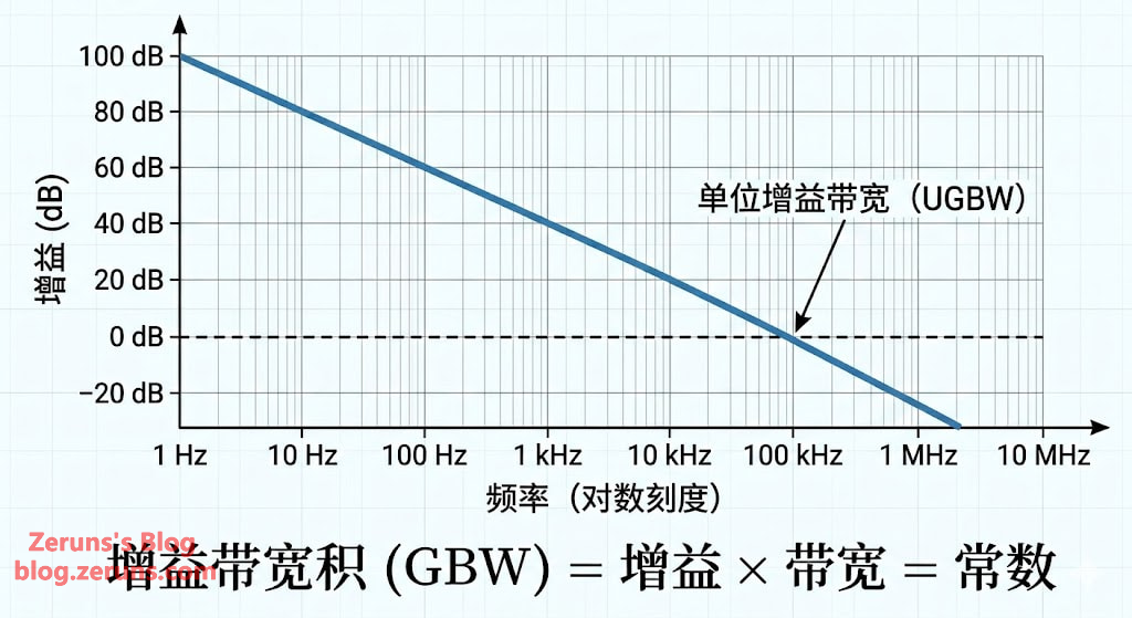
| Unity Gain Bandwidth UGBW | Unity Gain Bandwidth | Frequency at which open-loop gain drops to 1 (0dB). Above this frequency, the op-amp doesn't just fail to amplify, it actively attenuates. | ↑ Higher is better | General: 1~10 MHz |
| Gain Bandwidth Product GBW | Gain Bandwidth Product | The product of the op-amp's gain and bandwidth is constant. 10x Gain → Bandwidth drops to GBW/10. One of the most critical selection formulas. | ↑ Higher is better | 1~100 MHz |
| Closed-Loop -3dB Bandwidth | Closed-Loop -3dB Bandwidth | The frequency at which closed-loop gain drops to 0.707x (-3dB) its low-frequency value. | ↑ Higher is better | Depends on gain setting and GBW |
| Full Power Bandwidth FPBW | Full Power Bandwidth | The highest frequency capable of outputting a full-scale sine wave. \text{FPBW} = \frac{SR}{2\pi \cdot V_{max}} | ↑ Higher is better | Depends on SR and output swing |
12. 🔧 Hands-On Lab: Build Your First Op-Amp Circuit on a Breadboard
Watching ten times is not as good as doing it once. Here are two beginner-friendly experiments. All materials combined will cost less than $5.
12.1 Bill of Materials (BOM)
| Item | Specification / Model | Qty | Notes |
|---|---|---|---|
| Breadboard | 830 tie-points | 1 | Basic model is fine |
| Op-Amp Chip | LM358 (DIP-8 package) | 2 pcs | Dual op-amp, single-supply friendly, great for beginners |
| Resistors | 1\text{k}\Omega, 10\text{k}\Omega (1/4W) | 5 ea | Carbon film is fine, 5% tolerance is enough |
| Potentiometer | 10\text{k}\Omega adjustable resistor | 1 | Used to generate variable input voltage |
| Ceramic Caps | 0.1\mu\text{F} (104) | 4 pcs | For decoupling |
| Power Supply | 9V Battery + clip, or Adjustable DC supply | 1 set | Single supply 9V |
| Multimeter | Digital Multimeter | 1 | For measuring voltage |
| Jumper Wires | Male-to-Male (Dupont cables) | Varies |
12.2 Experiment 1: Voltage Follower
Goal: Verify "Output = Input", experience the function of a buffer.
Steps:
- Connect LM358's V_{CC} (Pin 8) to 9V, and GND (Pin 4) to ground. Don't forget to put a 0.1\mu\text{F} decoupling capacitor in parallel between the V_{CC} pin and ground!
- Use the center tap (wiper) of the potentiometer to generate an adjustable voltage between 0~9V, and connect it to the non-inverting input (Pin 3).
- Connect the output terminal (Pin 1) directly back to the inverting input (Pin 2) using a jumper wire.
- Use the multimeter to measure the input (Pin 3) and output (Pin 1) voltages respectively.
Expected Results: As you rotate the potentiometer, the output voltage consistently tracks the input voltage. If it doesn't follow, check:
- Is the op-amp powered?
- The LM358 is not a rail-to-rail output op-amp. The highest output voltage can only reach approx. V_{CC} - 1.5\text{V} (around 7.5V), and lowest around 0V.
12.3 Experiment 2: Non-Inverting Amplifier (2x Gain)
Goal: Verify V_O = V_I \times (1 + R_2/R_1).
Steps:
- Keep the basic power connections from Experiment 1.
- Connect R_2 = 10\text{k}\Omega between the output (Pin 1) and the inverting input (Pin 2).
- Connect R_1 = 10\text{k}\Omega from the inverting input (Pin 2) to ground.
- The non-inverting input (Pin 3) remains connected to the potentiometer's variable voltage.
Expected Results: Gain = 1 + 10\text{k}/10\text{k} = 2. Input 1V → Output approx. 2V; Input 2V → Output approx. 4V.
Advanced Variation: Swap R_2 for a 20\text{k}\Omega resistor and verify the gain changes to 1 + 20\text{k}/10\text{k} = 3.
12.4 Experiment 3 (Optional Challenge): Inverting Amplifier
- Ground the non-inverting pin (Pin 3).
- Connect the input signal via R_1 = 10\text{k}\Omega to the inverting pin (Pin 2).
- Bridge R_2 = 10\text{k}\Omega across the output (Pin 1) and the inverting pin (Pin 2).
Note: An inverting amplifier produces a negative output (relative to ground). If you use a single 9V supply, the op-amp cannot output a true negative voltage—so measuring the output might show approx. 0V (since it tries to go below 0V but hits the negative rail). You can connect the non-inverting pin to a V_{CC}/2 (approx. 4.5V) reference voltage to "lift" the operating point and verify the inverting amplification relationship.
12.5 Lab Safety Reminders
- The LM358 is a single-supply op-amp. Never apply negative voltage lower than -0.3V, or you might fry the chip.
- Before soldering or swapping components, disconnect the power—working on live circuits is the #1 reason beginners fry chips.
- If the circuit "isn't working," use your multimeter to probe the voltage on every pin and compare it to your expectations. 90% of issues stem from wiring mistakes or forgetting to power the chip.
Appendix: Classic Op-Amp Models Quick Reference
| Model | Type | Channels | Supply Range | GBW | SR | Characteristics | Est. Price |
|---|---|---|---|---|---|---|---|
| LM358 | General | Dual | 3V~32V (Single) | 1 MHz | 0.6 V/µs | Cheap, rugged, single-supply friendly | $0.10 |
| LM324 | General | Quad | 3V~32V (Single) | 1 MHz | 0.5 V/µs | Quad version, high cost-performance | $0.15 |
| TL074 | JFET Input | Quad | ±18V | 3 MHz | 13 V/µs | Low noise, high input impedance | $0.25 |
| NE5532 | Low-Noise BJT | Dual | ±3V~±20V | 10 MHz | 9 V/µs | Audio "God-tier" chip, ultra-low noise | $0.30 |
| MCP6002 | Low-Power RRIO | Dual | 1.8V~6V | 1 MHz | 0.6 V/µs | Battery-power top choice | $0.15 |
| OP07 | Precision | Single | ±3V~±18V | 0.6 MHz | 0.3 V/µs | Classic precision, ultra-low V_{OS} | $0.25 |
| OPA277 | Precision | Single | ±2V~±18V | 1 MHz | 0.8 V/µs | Ultra-low offset, low drift | $1.20 |
| AD8051 | High Speed | Single | 3V~12V | 110 MHz | 145 V/µs | High-speed voltage feedback | $0.75 |
💡 Selection Rules of Thumb:
- "Cheap and throwaway" → LM358 / LM324
- "Precision measurements, budget okay" → OP07 / OPA277
- "Wide voltage range, needs high impedance" → TL074 (JFET Input)
- "Needs to sound great" → NE5532
- "Low voltage battery power" → MCP6002
- "Lightning-fast high-speed" → AD8051
Conclusion: The op-amp is one of the core components in analog electronics. Once you master Virtual Short, Virtual Open, Negative Feedback, and a few basic topologies (Follower, Non-Inverting / Inverting Amplifiers), you can analyze and design the vast majority of entry-level circuits. However, theoretical knowledge is never enough—go buy a breadboard, some LM358s, and a handful of resistors, and do the experiments above. When you see the numbers on your multimeter matching the formula predictions with your own eyes, that sense of "wow, circuits really work like the theory says" is something no textbook can give you.
Happy soldering, and happy learning! 🔌
This article is aimed at beginners in electronics engineering, reorganizing op-amp fundamentals using practical analogies and hands-on perspectives. For deeper content (e.g., filter design, oscillators, PCB layout guides), refer to op-amp manufacturers' application notes (such as TI's "Op Amps for Everyone").
This article contains AI-generated content
Recommended Reading
- High Cost-Performance and Cheap VPS/Cloud Server Recommendations: https://blog.zeruns.com/archives/383.html
- Minecraft Server Hosting Tutorials: https://blog.zeruns.com/tag/mc/
- Discourse Forum Deployment Tutorial, Zero-Foundation Guide to Deploying a Discourse Open Source Community Website: https://blog.zeruns.com/archives/919.html
- 5G CPE Kunpeng C2000MAX Simple Unboxing & Review: https://blog.zeruns.com/archives/937.html
- Nanny-Level Tutorial on Deploying a Halo Blog with One Click via 1Panel: https://blog.zeruns.com/archives/858.html
- 【Open Source】SC8703-based Buck-Boost DCDC Adjustable Power Supply, Adjustable V/I, Supports PD Fast Charge Input: https://blog.zeruns.com/archives/929.html


Comment Section