


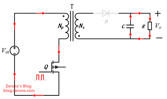
This article uses a 72-watt flyback power supply with a wide-range voltage input (24V, 3A output) as an example to demonstrate the calculation of circuit parameters and component selection. It also covers the calculation and winding methods for the flyback transformer.
The formulas in this article are referenced from online sources.
If you find any inaccuracies in this article, please feel free to point them out.
- 【Hardware Open Source】24V3A Flyback Switching Power Supply (Based on UC3842): https://blog.zeruns.com/archives/910.html
- Analysis, Comparison, and Selection Guide for Magnetic Components / Core Materials / Core Structures: https://blog.zeruns.com/archives/897.html
- Electronics / MCU Technology Exchange QQ Group: 2169025065
Flyback Power Supply Operating Parameters
First, you need to define the parameters for the flyback power supply you intend to design.
| Parameter | Value |
|---|---|
| Rated Input Voltage V_{acnom} | 220VAC |
| Minimum Input Voltage V_{acmin} | 85VAC |
| Maximum Input Voltage V_{acmax} | 265VAC |
| Line Frequency f_L | 50Hz |
| Output Voltage V_{out} | 24V |
| Output Current I_{out} | 3A |
| Operating Frequency f_s | 150kHz |
| Design Efficiency η | 85% |
The operating frequency of a flyback power supply is typically defined by the designer based on specific application requirements, rather than being a fixed value. Increasing the operating frequency can significantly reduce the size and weight of the transformer, output filter inductor, and capacitor, thereby minimizing the overall power supply dimensions. This is because high-frequency operation allows for the use of smaller magnetic components and capacitors. However, a higher frequency also leads to increased switching losses, which can reduce efficiency, exacerbate heat generation, and necessitate more complex thermal management. Therefore, selecting the frequency requires a careful trade-off between size, efficiency, cost, and thermal considerations.
The typical operating frequency range is from 20 kHz to 500 kHz, with 50 kHz to 200 kHz being the most common range. This strikes a good balance between size reduction and loss control. For designs exceeding 300 kHz, the crossover losses of conventional silicon-based switches (like MOSFETs) become significantly higher. In such cases, wide-bandgap semiconductor switches, such as Gallium Nitride (GaN) or Silicon Carbide (SiC), are typically required to reduce losses and maintain high efficiency.
Single-Phase Rectifier and Filter Circuit Calculation
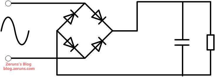
Calculation of Rectifier Bridge Diode Voltage Rating:
The DC bus voltage after rectification and filtering is typically close to the peak voltage of the AC input. The peak voltage of an AC signal is \sqrt{2} times its RMS value. Therefore, the reverse voltage rating of the rectifier bridge diodes must be greater than \sqrt{2} times the RMS value of the maximum input voltage.
Additionally, to account for grid surges and voltage fluctuations, a margin factor K_{bri} (typically 1.5) is usually applied. This gives us:
Therefore, the rated reverse voltage of the rectifier bridge diodes should be at least 562 V.
Input Power:
Calculation of Rectifier Diode Current Rating:
Maximum input current for a single diode in the rectifier bridge (since the diodes in a bridge conduct in pairs, the total current is divided by 2):
Similarly, to account for grid surges and voltage fluctuations, the same margin factor K_{bri} (typically 1.5) is applied. This results in:
Thus, the rated current for a single diode in the rectifier bridge should be at least 0.747 A.
Based on the calculations above, the MSB40M rectifier bridge is selected for this design. It has a rated voltage of 1000V and a rated current of 4A, which meets the calculated requirements.
Input Filter Capacitor Calculation:
There is an empirical formula for selecting the input capacitor of a flyback power supply:
For a single 220VAC input, the input capacitor C_{in} is typically chosen at 1-2μF/W.
For a universal 85VAC-265VAC input, the input capacitor C_{in} is typically chosen at 2-3μF/W.
Using this empirical formula, the filter capacitor is calculated as:
Therefore, based on the calculation, a 150μF electrolytic capacitor can be selected.
Selection of Input Filter Capacitor Voltage Rating:
It should generally be higher than the peak voltage of the AC input. For example, with V_{busmax} being 374.77V in this case, a 400V capacitor would be suitable. A 450V capacitor could also be used.
Flyback Transformer Calculation
To leave some margin, the minimum input voltage V_{busmin} is set to 110V.
Define the reflected voltage V_{OR} (the voltage induced on the primary winding when the switching transistor turns off and the magnetic field energy is released) as 100V. 100V is a typical engineering value for flyback power supply designs with wide input voltage ranges (e.g., 110V/220V AC).
Define the drain-source voltage drop of the primary MOSFET when it turns on as V_{ds} = 4V.
Calculate the Maximum Duty Cycle: (This can also be estimated empirically as 0.45 without calculation, as the duty cycle for a flyback supply generally does not exceed 0.5)
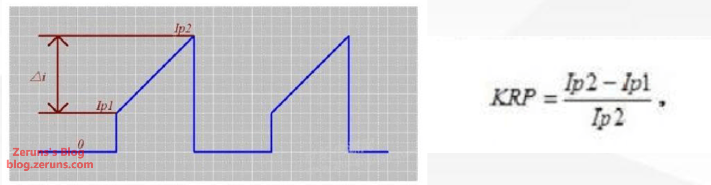
Calculate the Primary Peak Current:
- The input average current is:
- Assuming a ripple factor K_{RP} (ratio of ripple current I_R to peak current I_P) of 0.8 for CCM (Continuous Conduction Mode), the primary peak current I_P is calculated as:
Calculate the Transformer Magnetizing Inductance:
- Using the formula for the magnetizing inductance of a flyback transformer, the primary-side magnetizing inductance L_P is calculated as:
Calculate the AP Value and Select the Transformer Core Based on It:
The Core Area Product, AP = Aw * Ae (the product of the core's window area Aw and its effective cross-sectional area Ae).
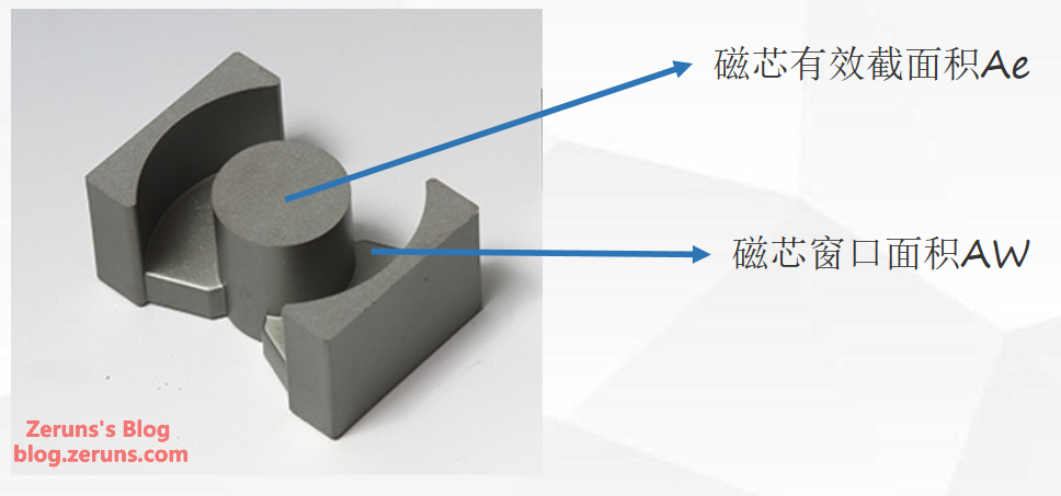
- With a transformer window fill factor K_o of 0.4, a current density coefficient K_j of 3.95, and a flux density B_w of 0.2T, the minimum required A_P value for the core is calculated as:
- The selected core's A_P value is typically more than twice the calculated design value. Here, I choose a PQ2620 core for the transformer. Consulting the core's datasheet, its A_P value is 0.7188\mathrm{~cm}^{4}.
Why is the Flux Density B_w Set to 0.2T?
1. To Avoid Core Saturation
- Core Saturation: When the flux density exceeds the material's saturation flux density ( B_{\text{sat}} ), the core loses its magnetic permeability, and its inductance drops sharply, leading to transformer failure.
- Ferrite Core Characteristics: The B_{\text{sat}} for common switching power supply cores (like PC40, PC44, PC95) is approximately 0.3–0.39 T at 100°C.
- Safety Margin: Setting B_w = 0.2 \, \text{T} (about 50–70% of B_{\text{sat}} ) provides a margin for the following factors:
- B_{\text{sat}} decreases at higher temperatures (the B_{\text{sat}} of ferrite cores decreases as temperature rises).
- Flux offset caused by the DC bias current.
- Increased peak current due to input voltage fluctuations or load transients.
2. To Control Core Loss
- High-Frequency Loss: Switching power supplies operate at high frequencies (typically >20 kHz). Core loss (hysteresis loss + eddy current loss) increases exponentially with flux density.
- Loss Optimization: Experience shows that when B_w is in the 0.1–0.25 T range, a good balance between core loss and copper loss can be achieved, resulting in higher overall efficiency. 0.2 T is a common compromise within this range.
Calculate the Primary and Secondary Turns:
V_F is the forward voltage drop of the output rectifier diode, typically taken as 0.7V.
- Based on the conservation of magnetic flux (Volt-second balance) between the primary and secondary sides, the primary-to-secondary turns ratio N_{PS} is calculated as:
- To prevent the transformer from saturating, the operating maximum flux density B_{max} is chosen as 0.15T. For a PQ2620 core, the A_e value is 119 mm² (119 \times 10^{-6}\,\text{m}^2). The primary number of turns N_P is calculated as:
The flux linkage \Psi = N(\text{turns}) \times B(\text{flux density}) \times S(\text{area})
- Based on the transformer's primary-to-secondary turns ratio, the secondary number of turns N_S is calculated as:
- An additional winding is added to the flyback transformer to supply power to the control IC. The designed output voltage for this auxiliary winding V_{out1} is set to 15V. Based on the relationship between output voltage and turns ratio, the number of turns for the auxiliary supply winding N_{s1} is calculated as:
Calculate the Wire Diameter and Number of Strands for Primary/Secondary Windings:
- The primary RMS current I_{prms} is calculated as:
- The secondary RMS current I_{srms} is calculated as:
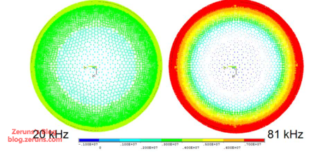
- The current in the transformer windings is high-frequency, which causes the skin effect. The current does not flow uniformly within the conductor but is concentrated near the conductor's "skin". The closer to the surface, the higher the current density, while the interior of the conductor carries very little current. The skin effect significantly reduces the effective cross-sectional area of the wire. Therefore, using multiple strands of thinner wire (such as Litz wire) instead of a single thick wire can effectively mitigate the skin effect. The calculated skin depth D_m (maximum diameter for a solid wire) is:
- The empirical current density is typically in the range of 4 to 6 A/mm². The selected wire diameter D_p and number of strands P_p for the primary winding are as follows:
- The calculated current density j_p for the primary winding is within the 4 to 6 A/mm² range.
- The selected wire diameter D_s and number of strands P_s for the secondary winding can be designed as follows.
- The calculated current density j_s for the secondary winding is:
Calculate Reference Coefficients:
- Calculate the coefficient of the total cross-sectional area of all windings relative to the transformer window area:
A window utilization factor K_w between 0.1 and 0.3 is generally considered appropriate.
Transformer Manufacturing Specification
Once the transformer parameters are calculated, a manufacturing specification can be created for the transformer vendor or for manual winding.
Winding Structure:
| Winding Layer | Terminals | Wire Spec | Turns | Winding Method |
|---|---|---|---|---|
| Layer 1 | 1-2 | Φ0.3mm (#28AWG) * 3 strands | 10 | Close-wound |
| Layer 2 | 5-6 | Φ0.3mm (#28AWG) | 3 | Close-wound |
| Layer 3 | 10-12 | Φ0.35mm (#26AWG) * 10 strands | 5 | Close-wound |
| Layer 4 | 2-3 | Φ0.3mm (#28AWG) * 3 strands | 10 | Close-wound |
Winding Details and Notes:
- Wind strictly according to the dot convention shown in the diagram. Pins 1, 5, and 10 are the dotted ends. Pay close attention to the dot orientation during winding.
- Pin 2 is the transition point for the sandwich winding.
- Apply tape between each layer. Add a margin of at least 2mm on the sides of layers 2 and 3.
- Apply sleeving to all lead-in and lead-out wires.
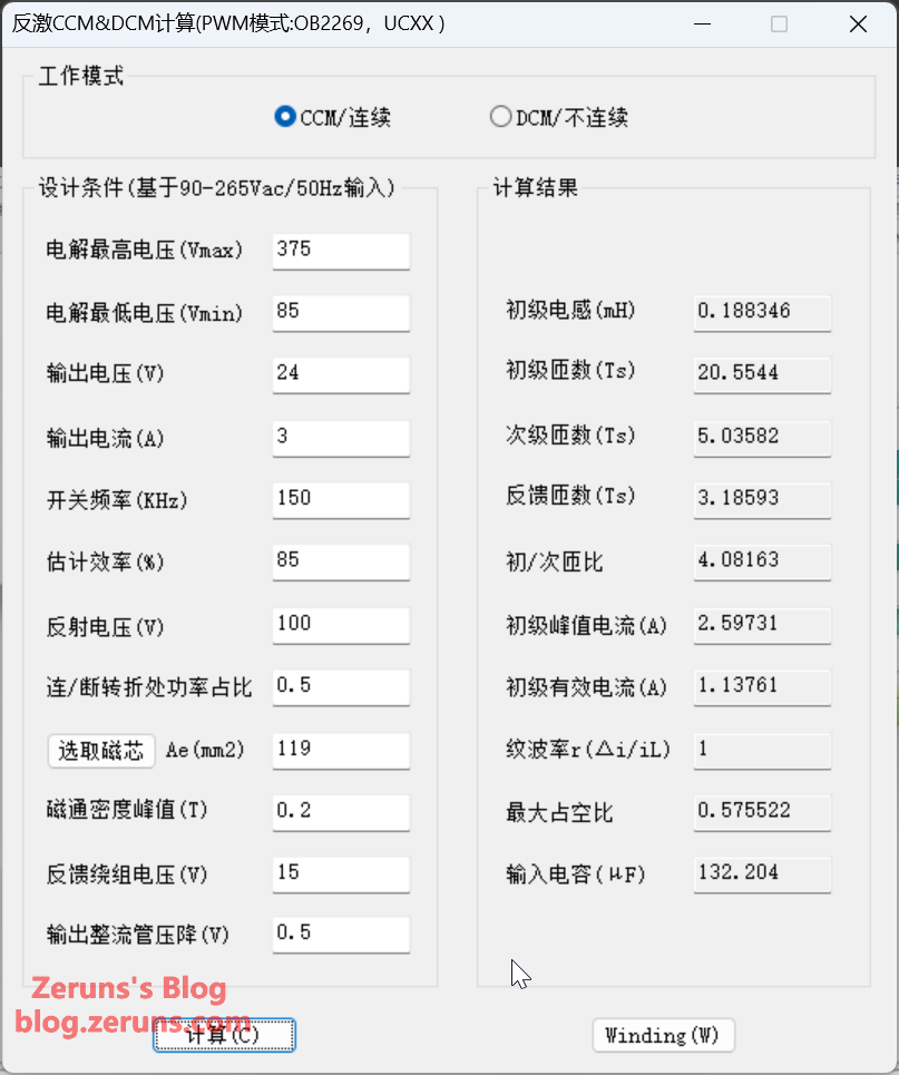
- Mark Pin 1 with a white dot for identification. Ensure an inductance of 156µH (measured between pins 1-3 @ 150kHz).
- Wind each layer evenly. If a layer is not full, wind it evenly with spacing (space-wound).
- Remove Pin 8.
Bobbin pinout, dot convention diagram, and winding structure are shown below:
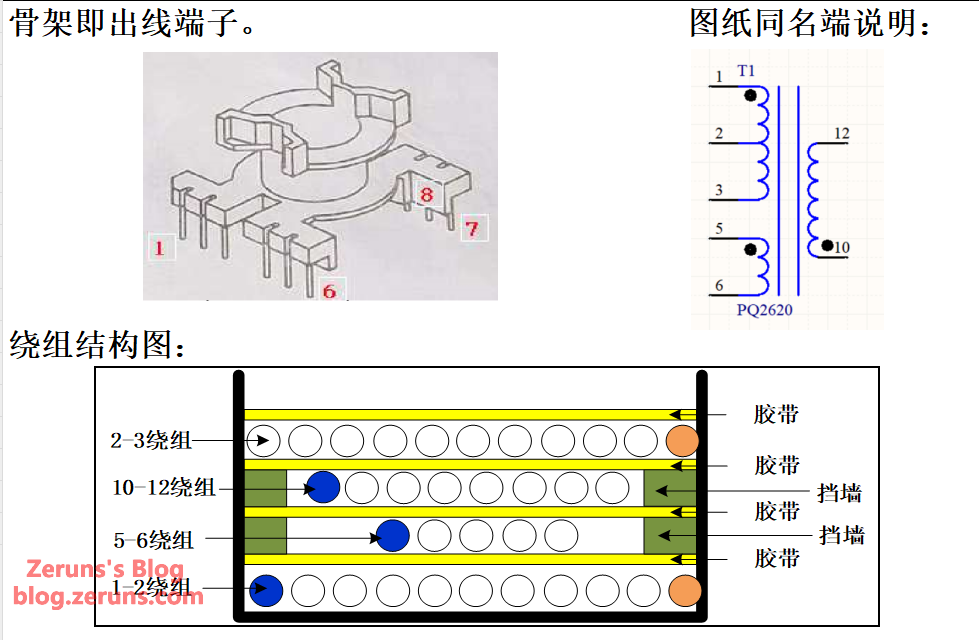
Transformer Related Information:
| Inductance | 1-3 pins: 156µH (ensure by grinding the center leg, measured @ 150kHz) |
|---|---|
| Core | PQ2620 (PC95/PC44 Ferrite) |
| Bobbin | PQ2620 Vertical Bobbin (6+6 pins) |
| Baseplate | None |
| Hipot Test | Pin 1 - Pin 10: 1500VAC (Frequency: 60Hz, Duration: 60s) |
| Temp. Class | CLASS F |
| Fixing Method | Fixed with tape. No potting or varnishing for now. |
| Lead-out Method | All lead-in and lead-out wires are to be sleeved with Teflon/Nylon insulation tubing. |
MOSFET Calculation and Selection
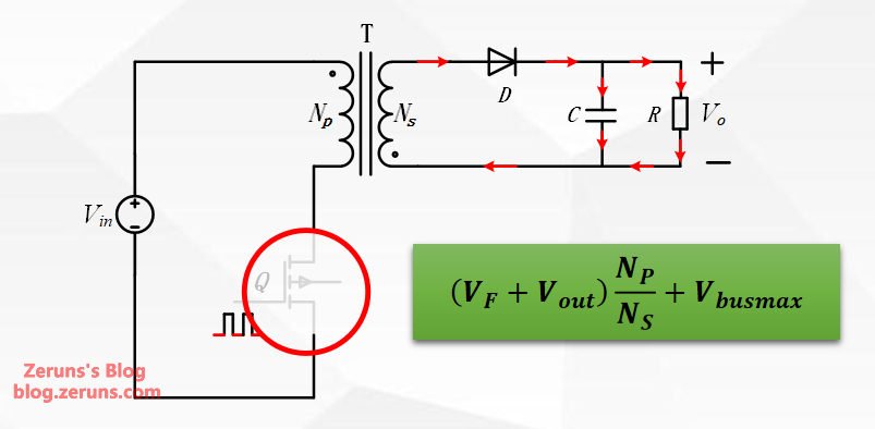
- During the MOSFET turn-off period, the plateau voltage across the MOSFET's drain and source is the sum of the input voltage and the voltage reflected from the secondary to the primary winding. This plateau voltage reaches its maximum when the input voltage is at its highest:
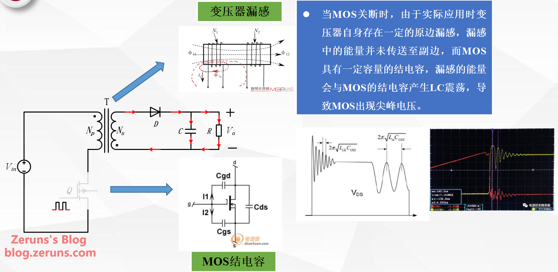
- When the MOSFET turns off, the primary leakage inductance of the transformer stores energy that is not transferred to the secondary side. This energy resonates with the MOSFET's junction capacitance, creating an LC resonance that causes a voltage spike on the MOSFET.
- In the design, this voltage spike must be prevented from damaging the MOSFET. Typically, a dedicated RCD clamp circuit is used to absorb this spike energy. At the same time, the selected MOSFET should have a sufficient voltage margin. In this design, a voltage margin of 1.5 times is used: K_{vmos}=1.3
- Therefore, the selected MOSFET must have a voltage rating that satisfies: V_{mos} \cdot K_{vmos} = 615.637\,\text{V}
- The MOSFET's RMS current is equal to the primary RMS current, which was previously calculated as I_{prms}=1.184\,\text{A}. A certain margin should be considered, so a MOSFET with a higher rated current should be selected.
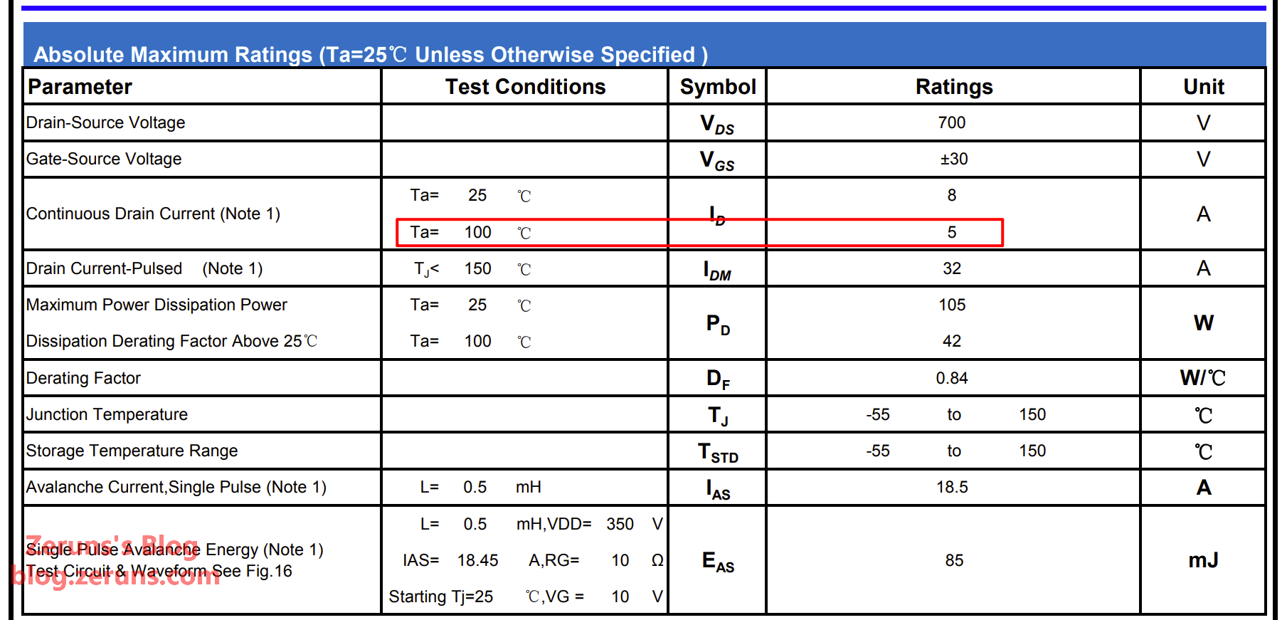
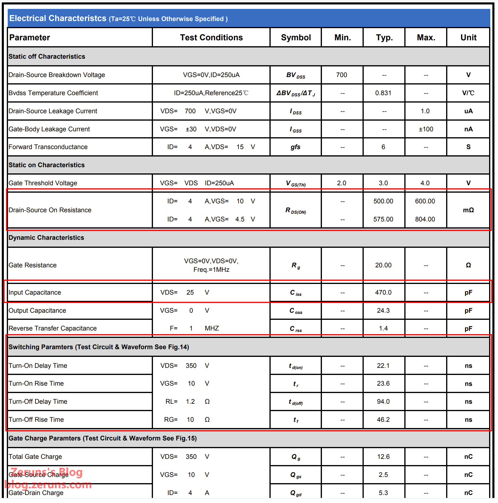
Based on the minimum voltage rating and the primary RMS current I_{prms}, the MOSFET selected for this design is the NJH65R600S, which has a rated voltage of 700V and a rated current of 8A, meeting the calculated requirements.
Note the table below: the rated current at 100°C must also be greater than the calculated primary RMS current.
In addition to voltage and current ratings, other key parameters for MOSFET selection are the on-resistance R_{DS(ON)} and input capacitance C_{iss}. Lower values for both are preferable. A lower R_{DS(ON)} results in lower conduction loss when the MOSFET is on. The input capacitance C_{iss} directly impacts switching loss and driving loss; a smaller C_{iss} leads to faster switching response, lower switching loss, and less charge/discharge current required from the driver circuit, thus reducing driving loss.
Output Diode and Capacitor Calculation and Selection
Output Diode Calculation and Selection:
- During the MOSFET on-time, the secondary rectifier diode is reverse-biased and blocks. The plateau voltage across it is the sum of the output voltage and the voltage reflected from the primary to the secondary winding. This plateau voltage reaches its maximum when the input voltage is at its highest. The reverse voltage across the diode when it is off is calculated as:
- When the diode is reverse-biased, the leakage inductance of the secondary winding resonates with the diode's junction capacitance, creating an LC resonance that causes a voltage spike when the diode turns off. When selecting a diode, a certain voltage margin should be chosen. In this design, a voltage margin of 1.5 times is used: K_{vdio} = 1.5
- Therefore, the selected diode must have a voltage rating that satisfies:
- Based on the minimum voltage rating calculated above and the secondary winding's RMS current, the diode selected for this design is the SBDD10200CT, which has a rated voltage of 200V and a rated current of 10A, meeting the calculated requirements.
- Additionally, it is important to use a Schottky diode. Schottky diodes have a low forward voltage drop (V_f), which significantly reduces conduction loss and improves power supply efficiency. They also have an extremely short reverse recovery time (typically < 10ns), which reduces energy loss and voltage oscillation during switching, making them especially suitable for high-frequency flyback power supplies.
- Alternatively, a synchronous rectifier (an integrated synchronous rectifier controller + MOSFET) can replace the Schottky diode. Synchronous rectification uses a MOSFET to replace the diode, controlled precisely by a controller. Its advantage lies in the extremely low on-resistance (R_{ds(on)}), which further reduces conduction voltage drop and loss, improving efficiency (especially in high-current output applications).
Output Capacitor Calculation and Selection:
- When the MOSFET turns on, the secondary diode is reverse-biased, and the capacitor supplies power to the load, causing the output voltage to decrease and form output voltage ripple.
- The capacitor current equals the load current, and the rate of voltage decrease across the capacitor is equal to the capacitor current divided by its capacitance.
- The ripple voltage is equal to this rate of voltage decrease multiplied by the primary MOSFET on-time, which is the same as the secondary diode's off-time.
- For switching power supplies in consumer electronics, the output voltage ripple ratio (the percentage of peak-to-peak ripple voltage to the output voltage) is typically required to be within 1% to 2%. For my 24V output, this means the ripple voltage should be between 0.24V and 0.48V. A lower ripple voltage is also acceptable but would require a larger capacitance. Here, I set \Delta V_{out} = 0.1\,\text{V} . Therefore, the output capacitance can be calculated as:
- This calculation is for an ideal capacitor with zero ESR. In practice, capacitors have a certain ESR, which increases the ripple. The ESR varies by capacitor model, so the selected value is typically higher than the theoretical one and should be finalized through testing.
- To reduce the ESR, multiple capacitors can be used in parallel. In this design, two 220uF/35V electrolytic capacitors are used in parallel. Solid capacitors (which have lower ESR than electrolytic capacitors) can be used as an alternative. Additionally, multiple MLCC capacitors (e.g., 1μF, 100nF) should be added in parallel to filter high-frequency noise.
RCD Snubber Circuit Analysis and Calculation
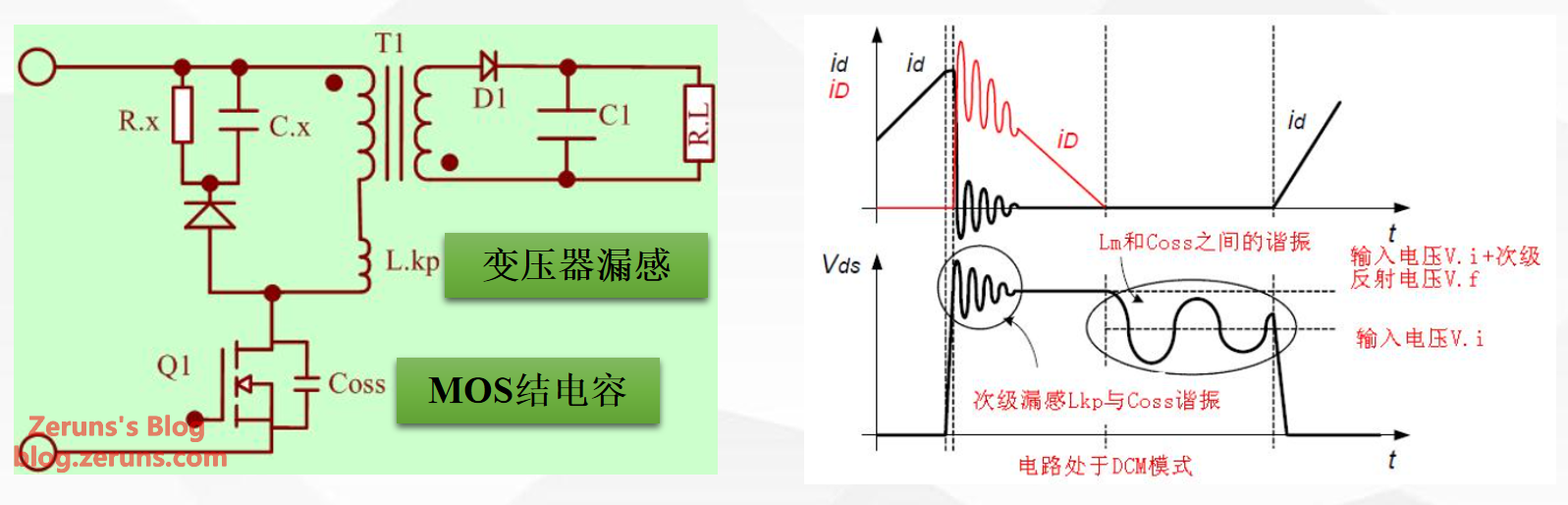
- The circuit may experience two oscillations. The first is primarily caused by the primary leakage inductance L_{kp} and the MOSFET's C_{oss} (output capacitance). The second is mainly caused by the oscillation between the magnetizing inductance (primary inductance) and the C_{oss} capacitance after the circuit's energy is depleted.
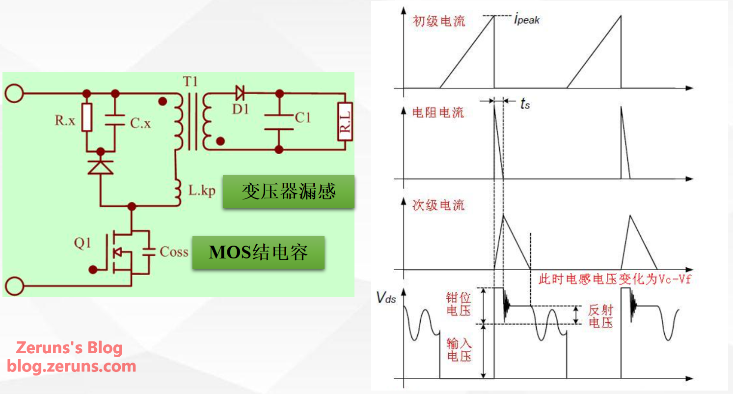
- After adding the RCD snubber circuit, when the voltage across the MOSFET exceeds the sum of the clamp capacitor voltage and the input voltage, the clamp diode conducts, and the clamp circuit begins to operate.
- Assume the transformer's primary leakage inductance L_k is controlled within 1% of the magnetizing inductance (primary inductance): L_k=1\% \cdot L_p=1.557uH (It is best to measure the actual primary leakage inductance after the transformer is produced and recalculate the following values using the measured value. Measurement method for primary leakage inductance: Short all windings except the primary, then measure the primary inductance with an LCR meter. The measured value is the primary leakage inductance.)
- The known maximum voltage of the switching transistor V_{dsmax} is 700V.
- Leaving some margin, the desired voltage on the clamp capacitor V_{clamp} is designed as:
- Calculate the clamp resistor R_c and clamp capacitor C_c using the standard RCD snubber calculation formulas:
- Meanwhile, calculate the power dissipated by the clamp:
- Select a 20kΩ clamp resistor and a 1nF clamp capacitor. Choose a 2W power resistor. Based on the voltage on the clamp capacitor, and considering the higher voltage during startup, a film capacitor with a 1kV voltage rating or a 1206 package MLCC can be chosen. Similarly, select a 1kV clamp diode FR107.
Downloads
If you don't want to calculate manually, you can use the Mathcad worksheet or SMPSKit software to perform the calculations. Download links are as follows:
- 123 Cloud Drive: https://www.123684.com/s/2Y9Djv-A3TdH
- Baidu Cloud Drive: https://pan.baidu.com/s/1USh47nHgYxjTzTJgo4DVTQ?pwd=xyxf Extraction Code: xyxf
Transformer Winding
This was also my first time winding a transformer, so the work isn't perfect. This is for reference only.
All windings must start from the dot-end pins and be wound in the same direction!
In the pictures below, I used both enameled wire (left) and Litz wire (right).
The diameter of the PQ2620 core is 14.5mm. Using the circumference formula L = \pi d, the length of one turn is calculated to be 45.53mm. Multiply this by the number of turns to get the required length for each winding, then add an extra ten or so centimeters of margin. Cut the enameled wire to this calculated length.
Layer 1: First, wind the first layer of the primary winding. Take three 0.3mm diameter enameled wires and wind them together starting from pin 1 of the transformer bobbin. Make 10 turns on the bobbin. (For the Litz wire, I used 0.1mm x 30 strands).
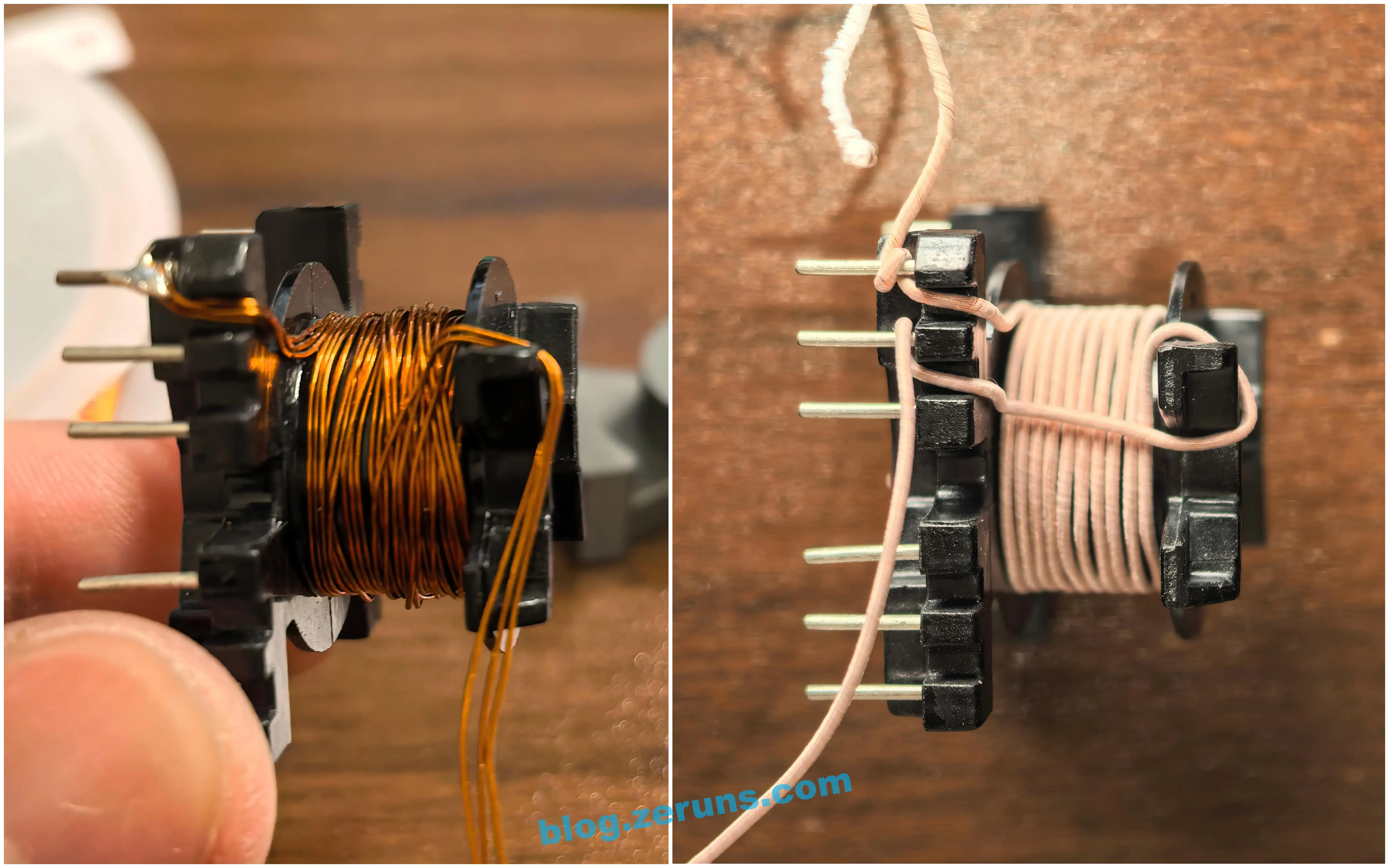
After finishing the first layer, route the wires upwards and wrap a layer of tape (use Mylar tape or polyimide tape). Then, route the wires vertically down to pin 2 and wrap two more layers of tape.
Layer 2: First, wind marging tape on both sides. Then, wind a single 0.3mm enameled wire starting from pin 5, making 3 turns in the same winding direction as the first layer, ending at pin 6. Finally, wrap two layers of tape. (For the Litz wire, I used 0.1mm x 10 strands).
Layer 3: First, wind marging tape on both sides. Then, take ten 0.35mm diameter enameled wires and wind them together starting from pin 10 of the transformer bobbin. Make 5 turns in the same winding direction as the first layer, ending at pin 12. Finally, wrap two layers of tape. (For the Litz wire, I used 0.1mm x 60 strands).
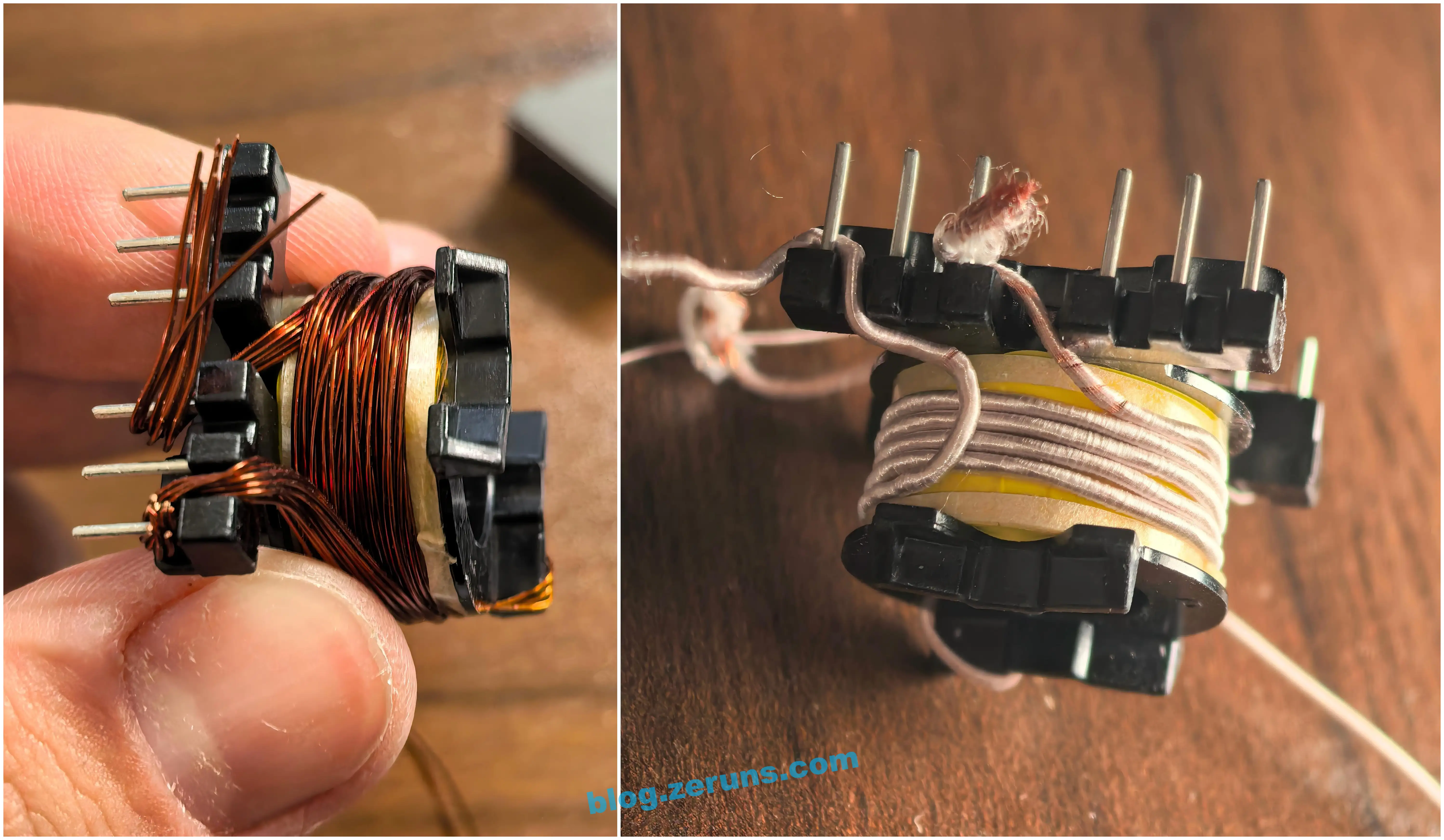
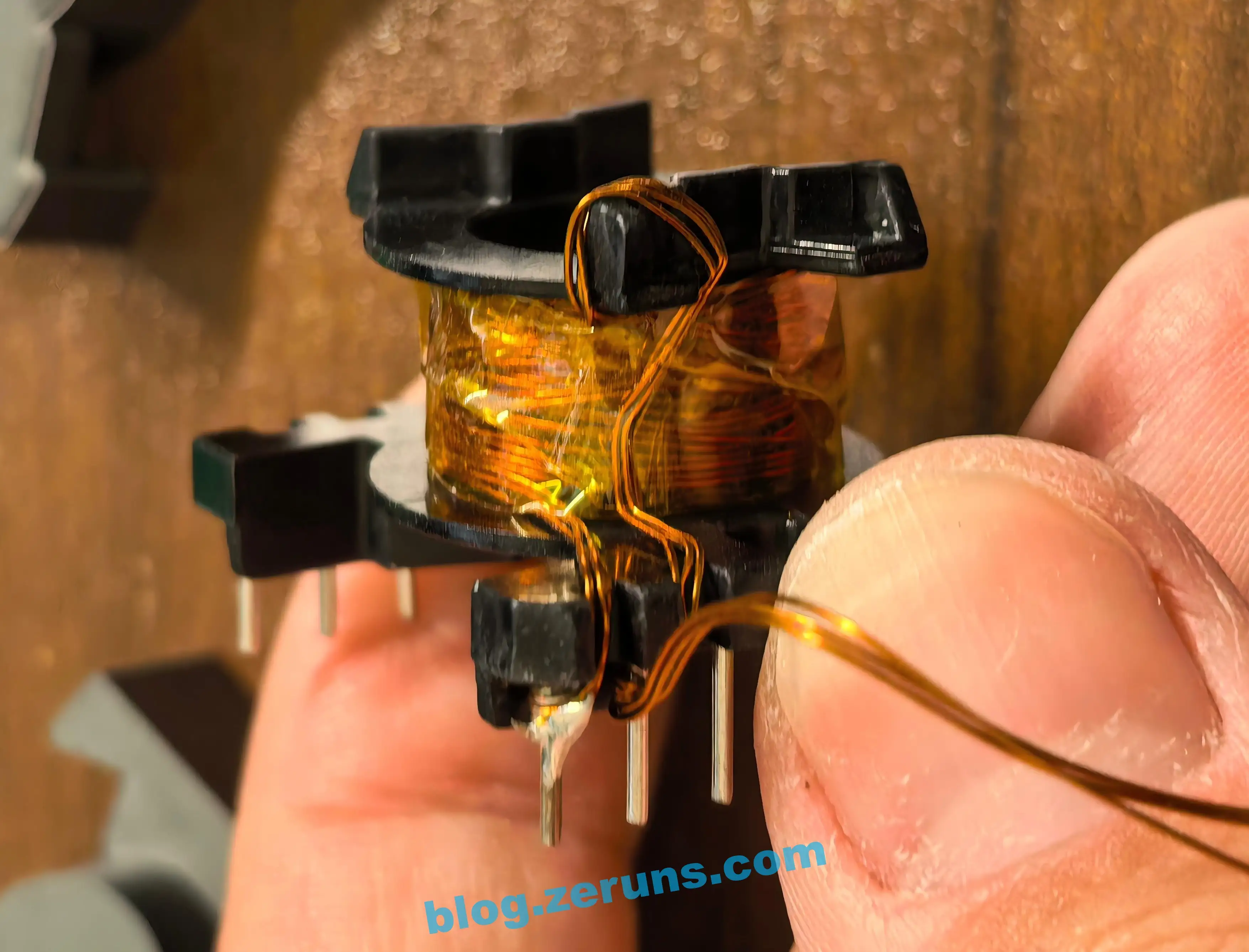
Layer 4: Continue winding the primary winding. Start from pin 2 and make 10 turns in the same winding direction as the first layer, ending at pin 3. It's best to route the wire vertically down after finishing. Finally, wrap two layers of tape.
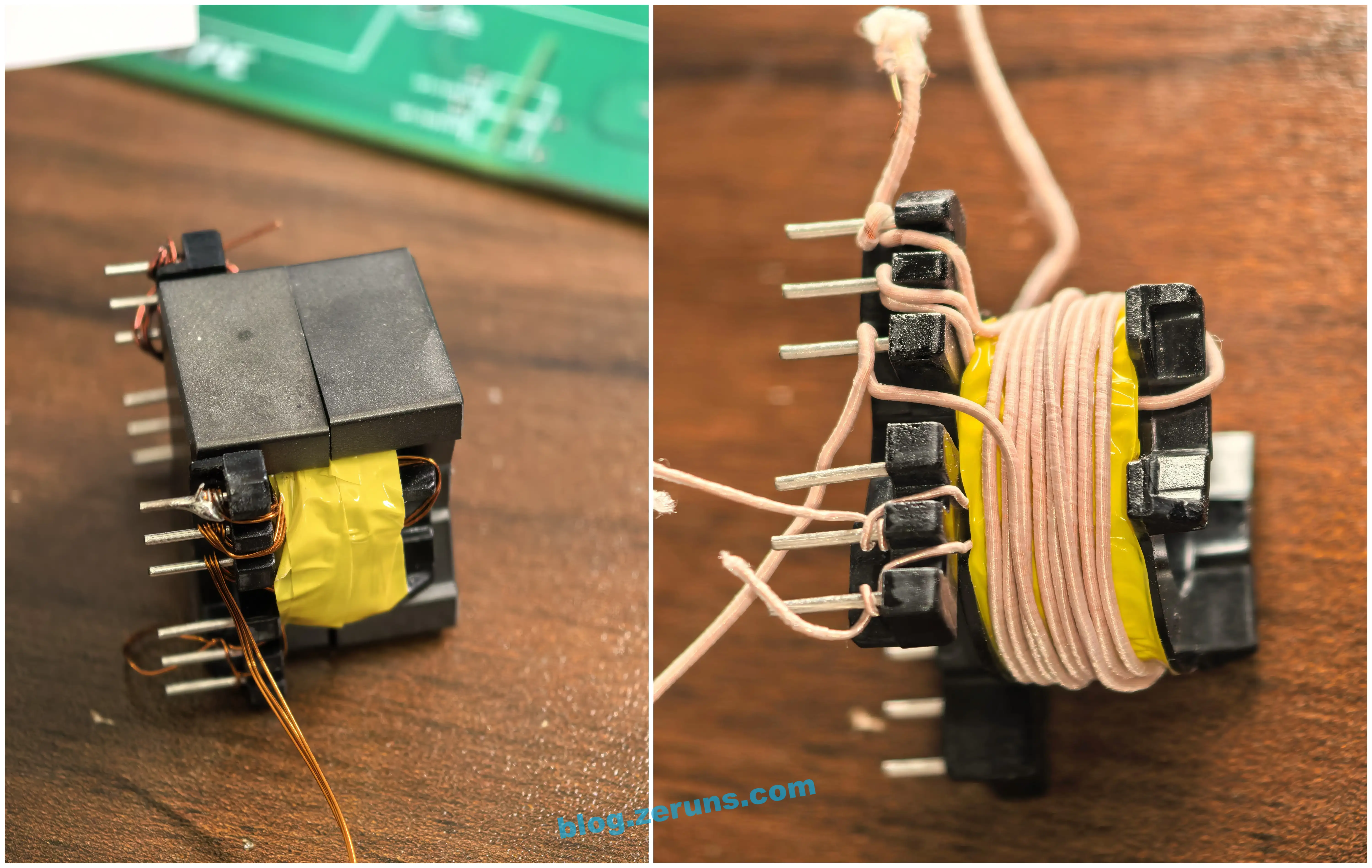
Next, solder all the enameled wires to their respective pins. You may need to scrape off the enamel coating with a blade for some wires before they can be tinned. For Litz wire, you can apply a hot soldering iron for a while to tin it.
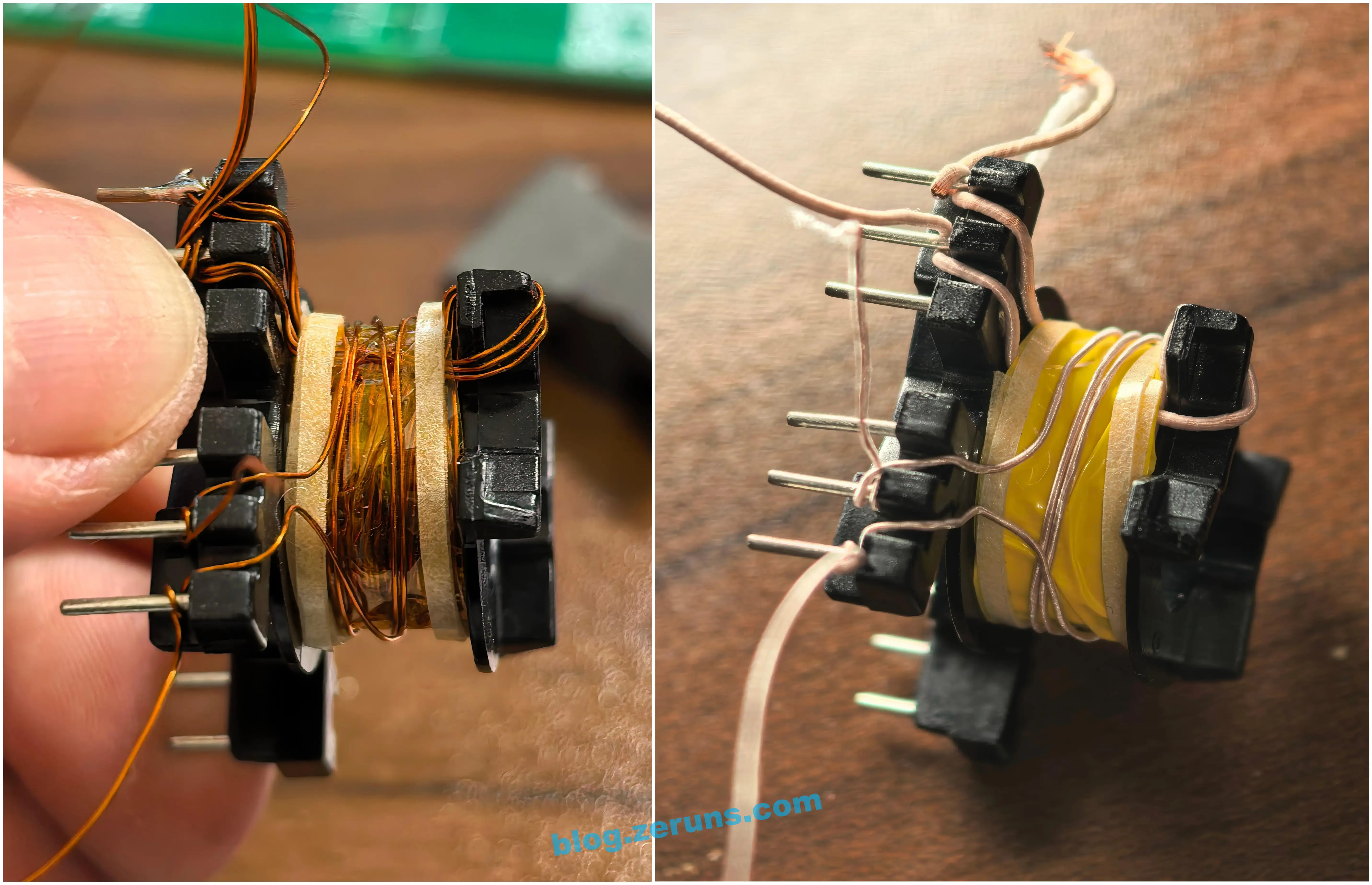
In a flyback switching power supply, the transformer needs to store the energy to be transferred during the cycle. To prevent magnetic saturation, an air gap is usually introduced into the core to alter the hysteresis loop, increasing the saturation flux density and thus the energy transferred per cycle. There are two common methods for creating an air gap: grinding it or shimming it, with shimming being the simpler method.
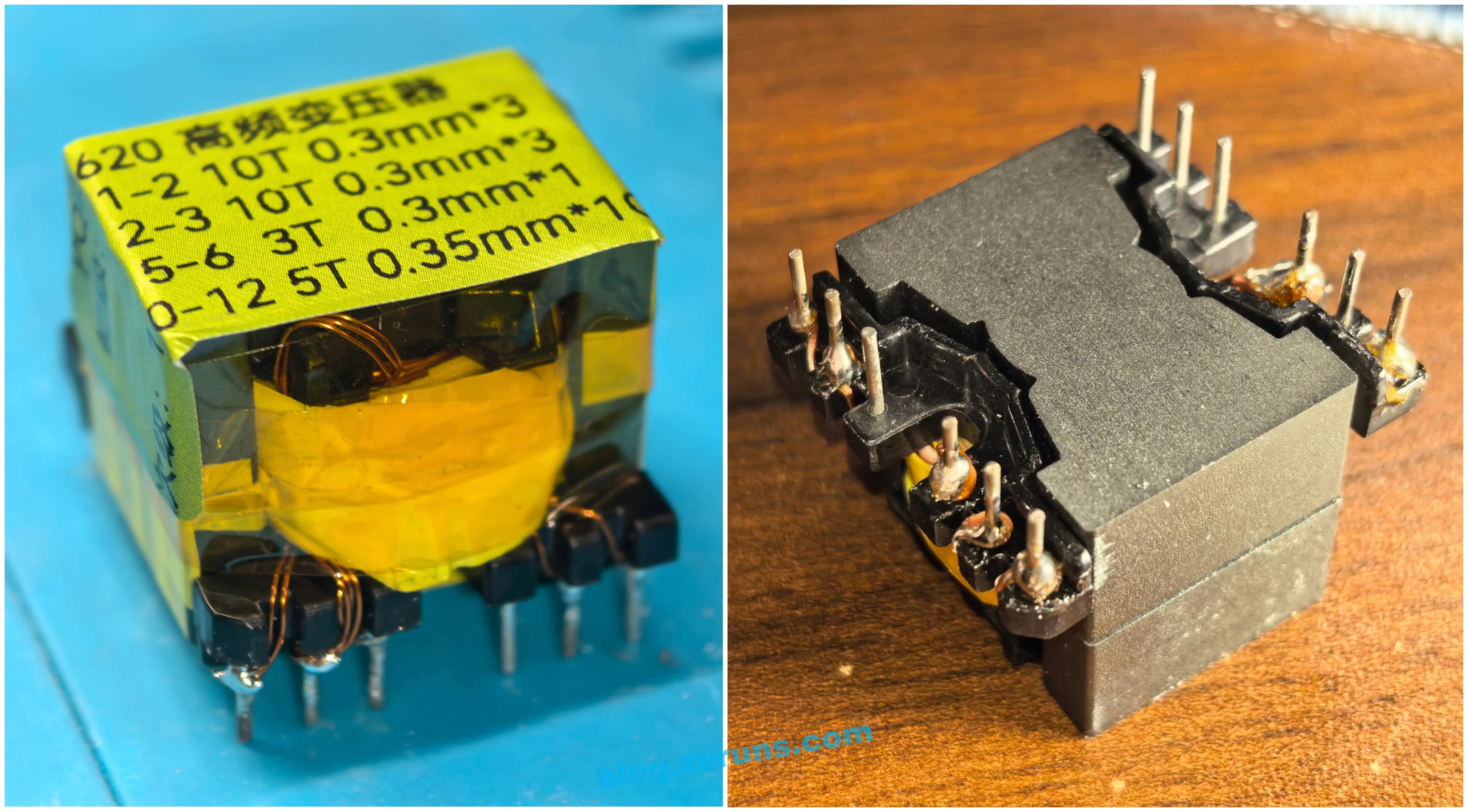
Finally, assemble the core halves, press them together firmly, and measure the primary winding inductance. If the inductance is much higher than the target value (156μH in my case), use a file or other grinding tool to grind the center post of the core (grinding an air gap). Measure after each small amount of grinding until the inductance is just slightly above the target value. Then, wrap the entire core tightly with tape.
Alternatively, you can use the shimming method. This involves placing a few layers of tape or other thin material between the core halves. Measure the inductance after adding each layer until it is just slightly above the target value. Then, wrap the entire core tightly with tape.
Shimming an air gap generally results in slightly higher leakage inductance compared to grinding.
After completion, measure again. The primary winding inductance of my transformer is 158.8μH.
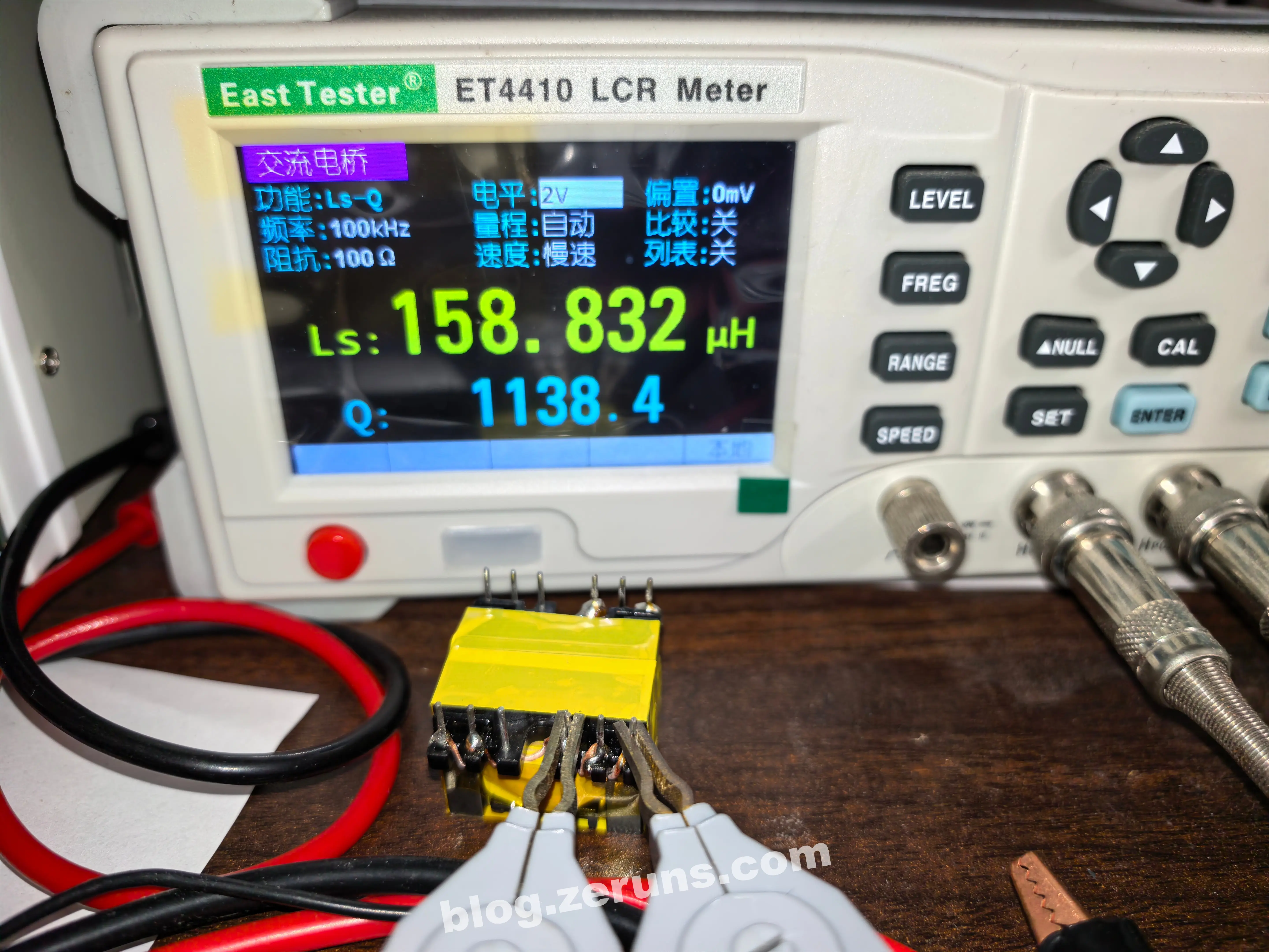
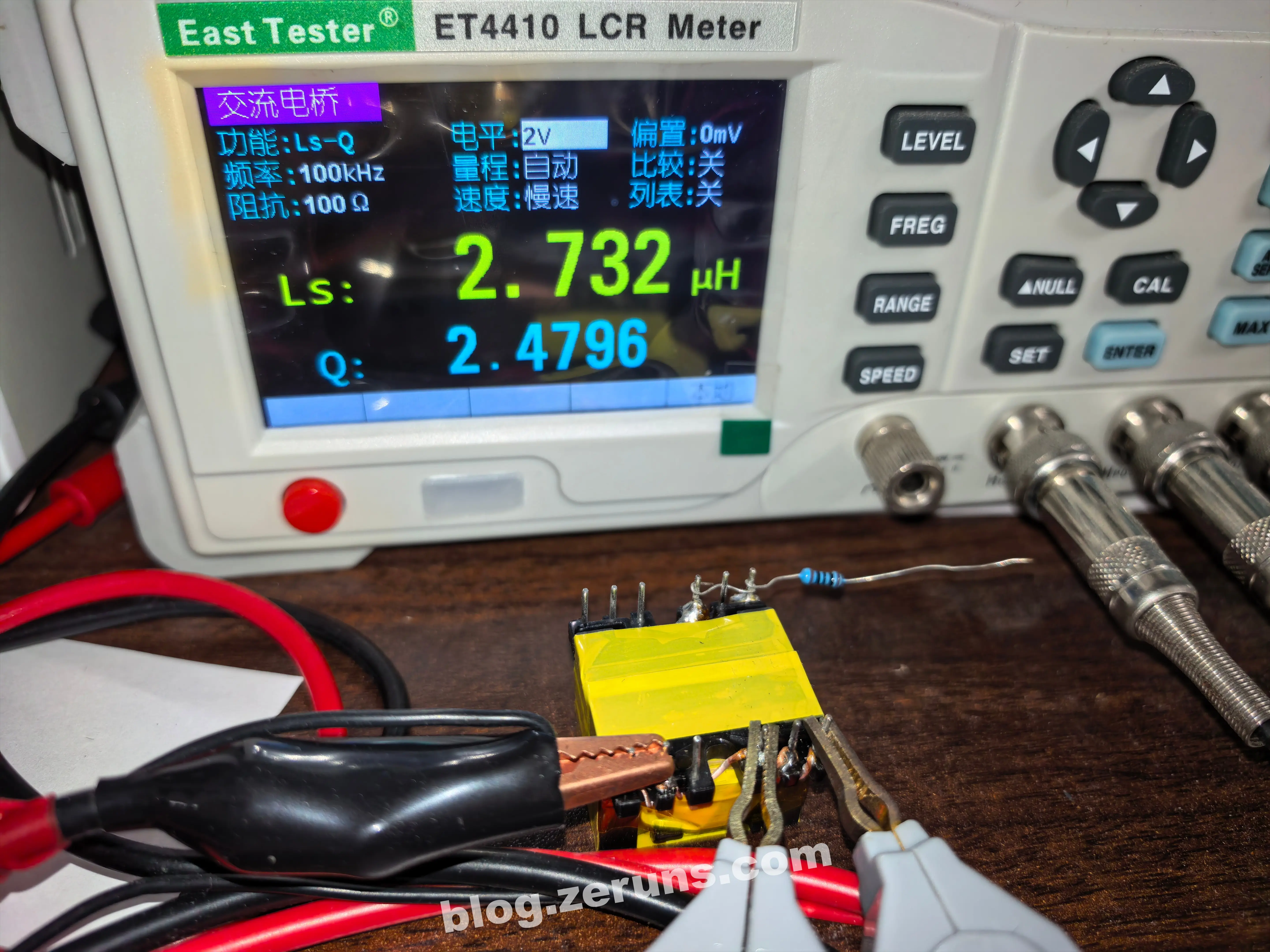
Measure the primary leakage inductance by shorting the other windings and then measuring the inductance of the primary winding. My measurement came out to 2.7μH, which is a bit high.
Recommended Open Source Projects
- I've open-sourced a three-phase power collector, which can conveniently monitor home electricity consumption: https://blog.zeruns.com/archives/771.html
- Open-sourced an STM32-based Synchronous Rectification Buck-Boost Digital Power Supply: https://blog.zeruns.com/archives/791.html
- LM25118 Automatic Buck-Boost Adjustable DCDC Power Module: https://blog.zeruns.com/archives/727.html
- Open-sourced a CH32V307-based Smart Electronic Load, an entry for the Embedded Systems Competition: https://blog.zeruns.com/archives/785.html
- EG1151 High-Power Synchronous Rectification Adjustable Buck-Boost Power Module (supports Type-C PD fast charging input) Open-sourced: https://blog.zeruns.com/archives/794.html
- Open-source 140W+65W Buck-Boost PD3.1 Fast Charging Module (2C+1A ports), IP6557+IP6538, 205W Desktop Charger: https://blog.zeruns.com/archives/801.html
- Open-source Type-C Hub with 4x 10Gbps USB-A ports + 2.5G Network Card + Card Reader: https://blog.zeruns.com/archives/868.html
Recommended Reading
- High Cost-Effective and Cheap VPS/Cloud Server Recommendations: https://blog.zeruns.com/archives/383.html
- Minecraft Server Setup Tutorial: https://blog.zeruns.com/tag/mc/
- Cross-Border E-commerce Independent Site Building Tutorial, WordPress Foreign Trade Website Guide: https://blog.zeruns.com/archives/889.html
- ZGRL-80 Photography Light Teardown and Circuit Design Analysis: https://blog.zeruns.com/archives/882.html
- MECHREVO Code10AI Laptop (Ultra7-255H) Simple Unboxing Review and Teardown: https://blog.zeruns.com/archives/895.html
- GL-RM1PE Simple Unboxing Review and Teardown, Enabling BMC Remote Management for a Regular PC: https://blog.zeruns.com/archives/900.html


Comment Section