


Open-sourcing a wide input voltage, 24V 3A output flyback switching power supply. This 72-watt design achieves a peak efficiency of 87.4% and is based on the UC3842 controller chip with synchronous rectification (UCC24612-1DB). It includes the complete calculation process for circuit and transformer parameters, schematics, PCB, PSIM simulation models, transformer manufacturing specifications, and more.
Foreword
📍This is my first time designing a flyback power supply. I welcome any feedback or suggestions for improvement from all the experts out there.
- Flyback Power Supply Parameter Calculation & Component Selection, Flyback Transformer Calculation & Winding Tutorial: https://blog.zeruns.com/archives/909.html
- Magnetic Components / Core Materials / Core Structures Analysis, Comparison, and Selection Guide: https://blog.zeruns.com/archives/897.html
🚀On a side note, I'm currently looking for a job. If any employers in Guangzhou, Foshan, or Shenzhen are hiring, please consider me. You can check out my open-source projects on my OSHWHub homepage: https://oshwhub.com/zeruns/works
▶Project Video Demo & Design Process Video: https://www.bilibili.com/video/BV1ES4GzQE19/
▶OSHWHub Open-Source Link: https://oshwhub.com/zeruns/24v3a-Flyback-Power-Supply-uc384x
▶Electronics/MCU Technical Discussion QQ Group: 2169025065
Download links are at the end of the article!
Warning: Building switching power supplies can be dangerous. I do not guarantee the correctness of any circuits, parameters, or formulas in this design. You are responsible for assuming all possible risks if you replicate or reference this project.
The estimated average cost for a small batch (20 units) is around 25 RMB (excluding PCB and transformer, based on component prices from LCSC Mall). Including the PCB and transformer, the total cost should not exceed 50 RMB.
Design Parameters
| Parameter | Value |
|---|---|
| Rated Input Voltage V_{acnom} | 220VAC |
| Minimum Input Voltage V_{acmin} | 85VAC |
| Maximum Input Voltage V_{acmax} | 265VAC |
| Line Frequency f_L | 50Hz |
| Output Voltage V_{out} | 24V |
| Output Current I_{out} | 3A |
| Operating Frequency f_s | 150kHz |
| Target Efficiency η | 85% |
PCB Dimensions: 100x55mm
PCB Specifications: Double-layer board, top layer for through-hole components, bottom layer for SMD components.
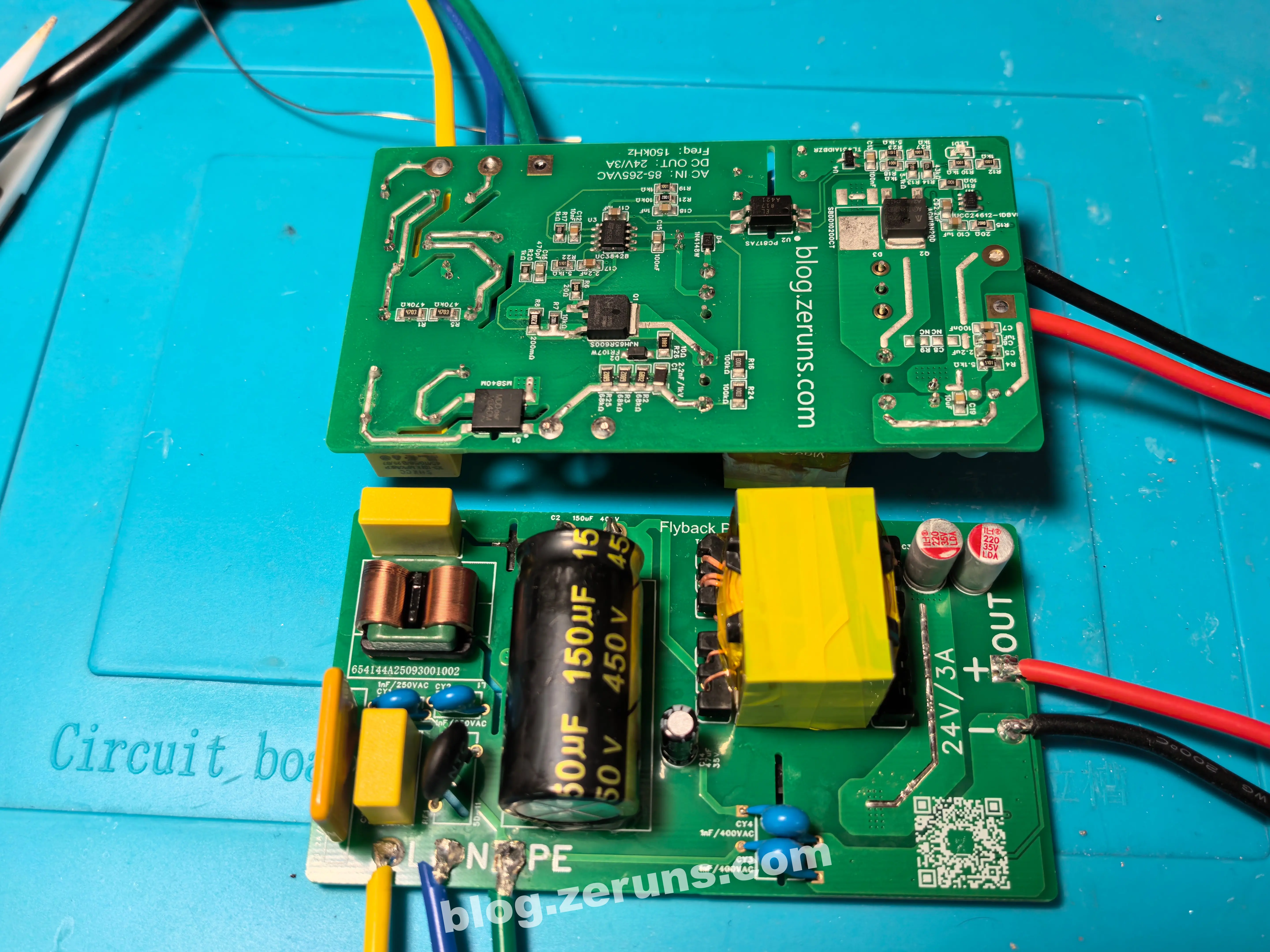
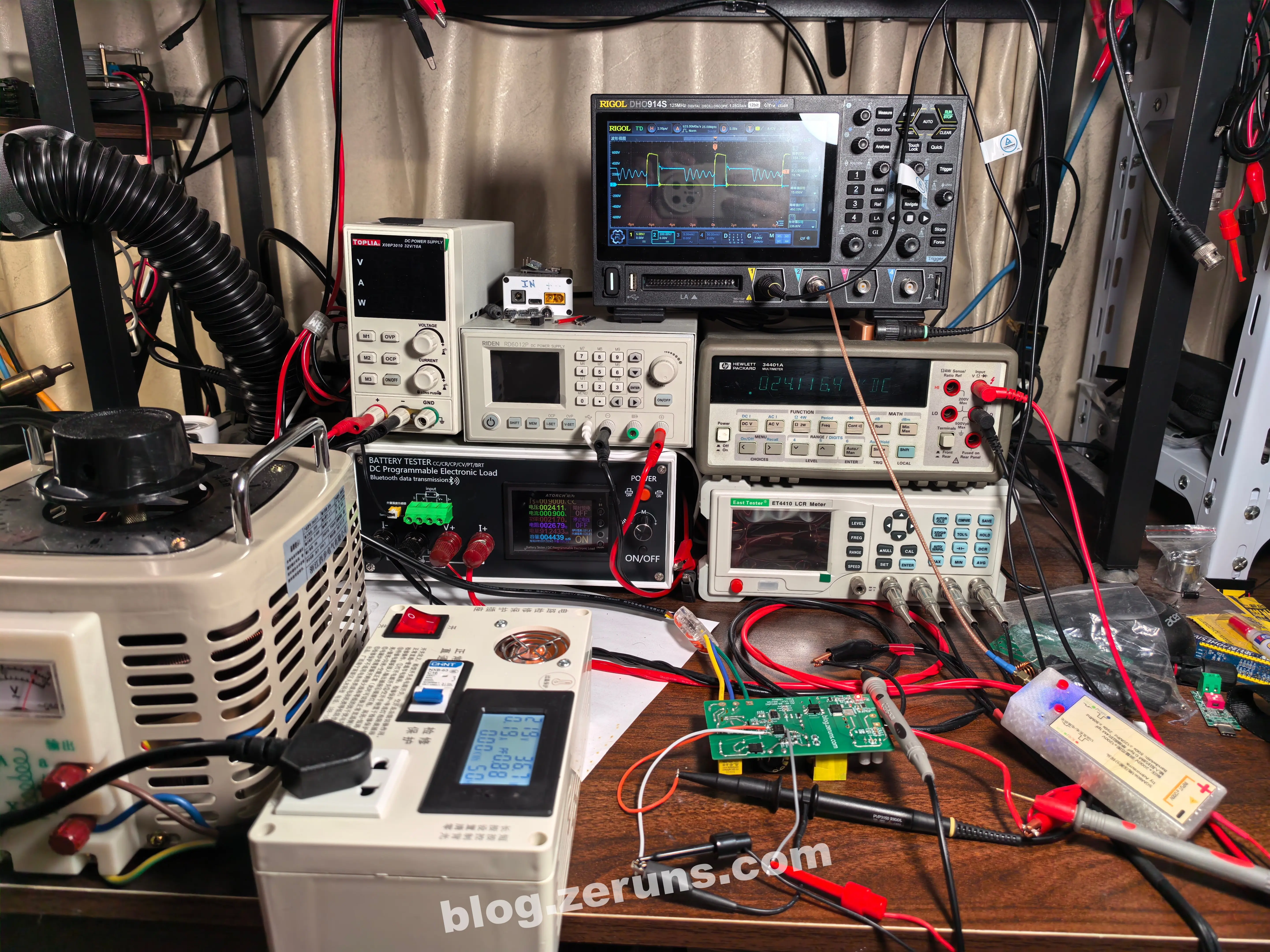
Physical Photos
The picture below shows the second version.
The picture below shows the first version, which had some issues and was prone to blowing MOSFETs. These issues were fixed in the second version shown above.
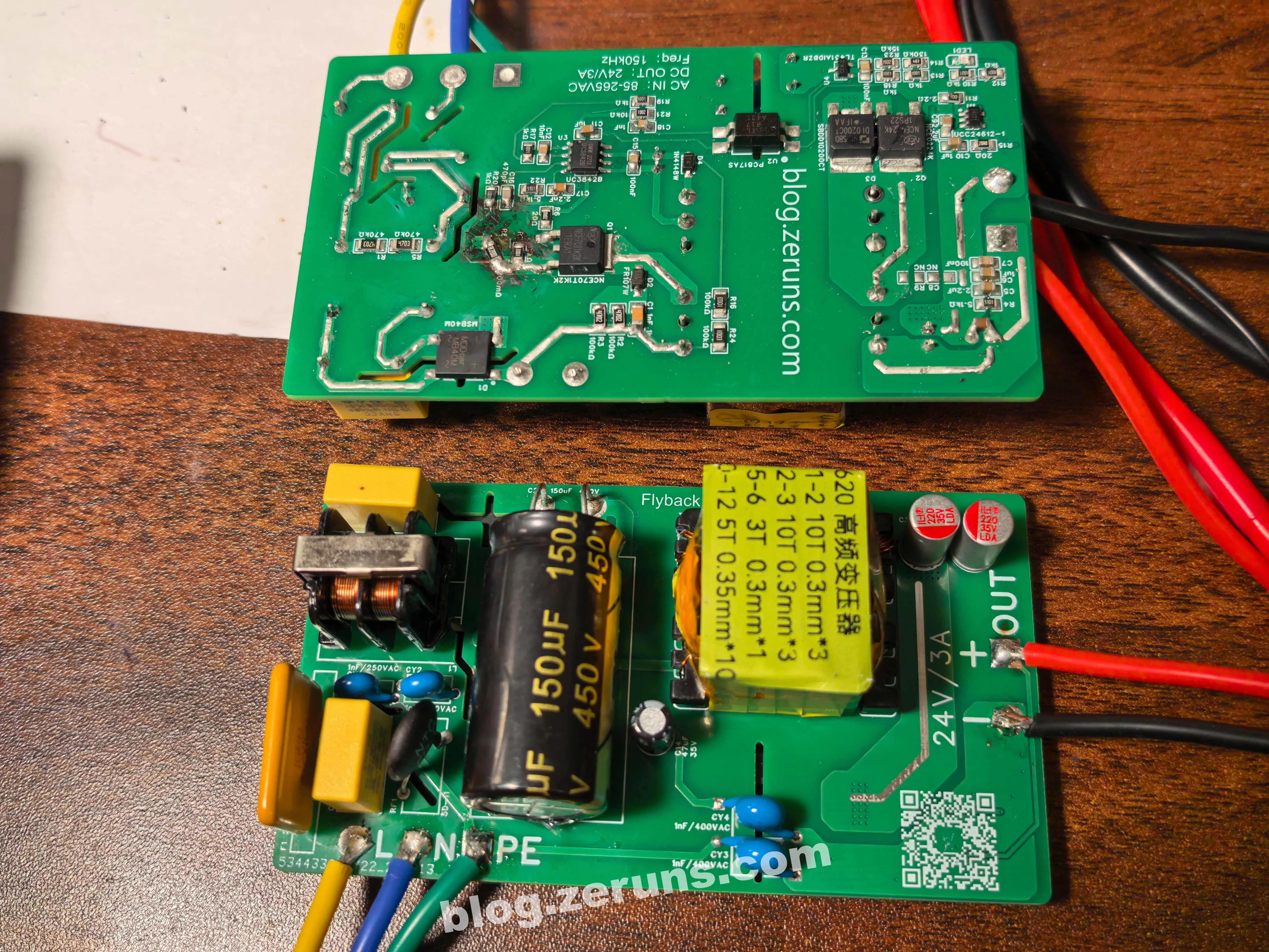
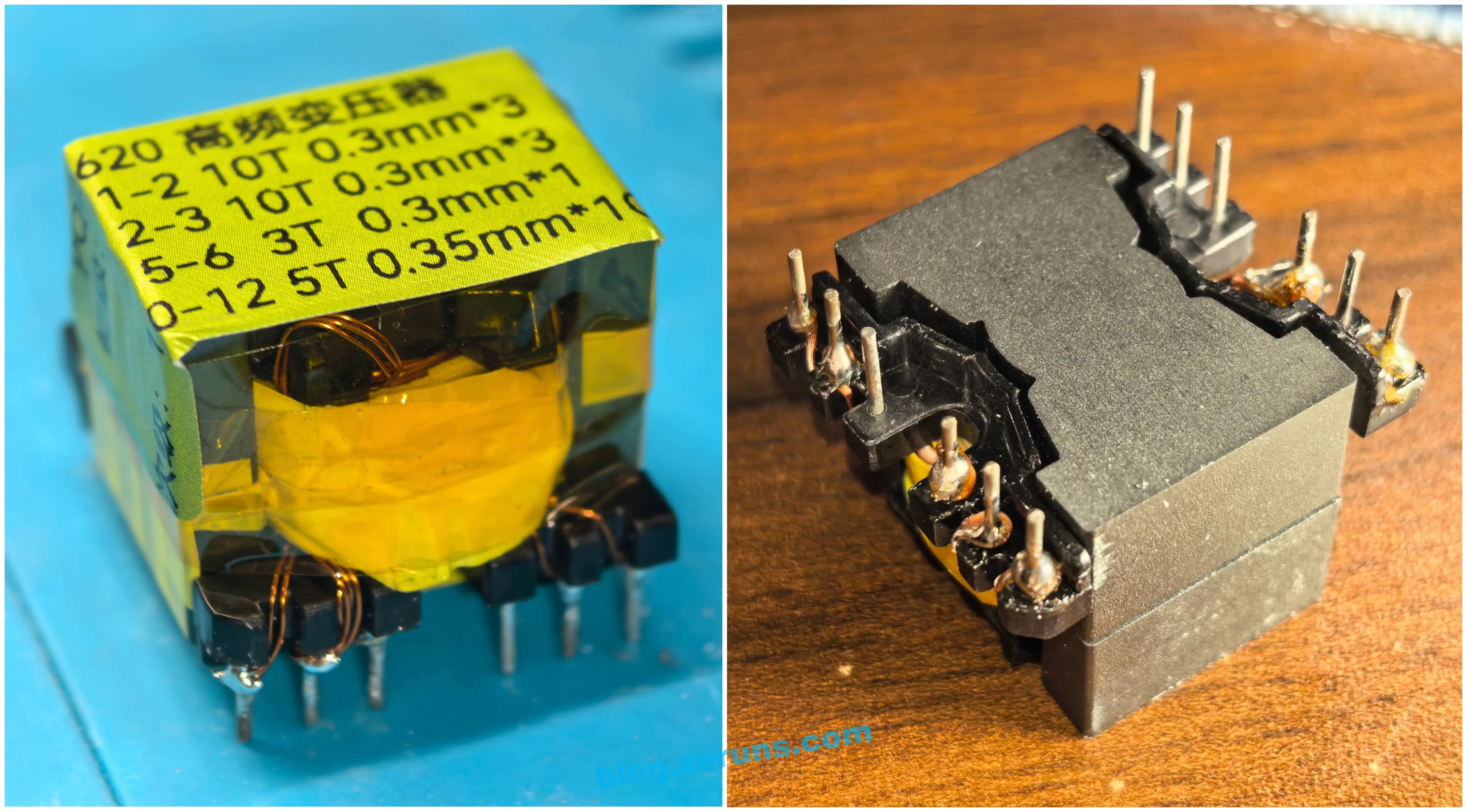
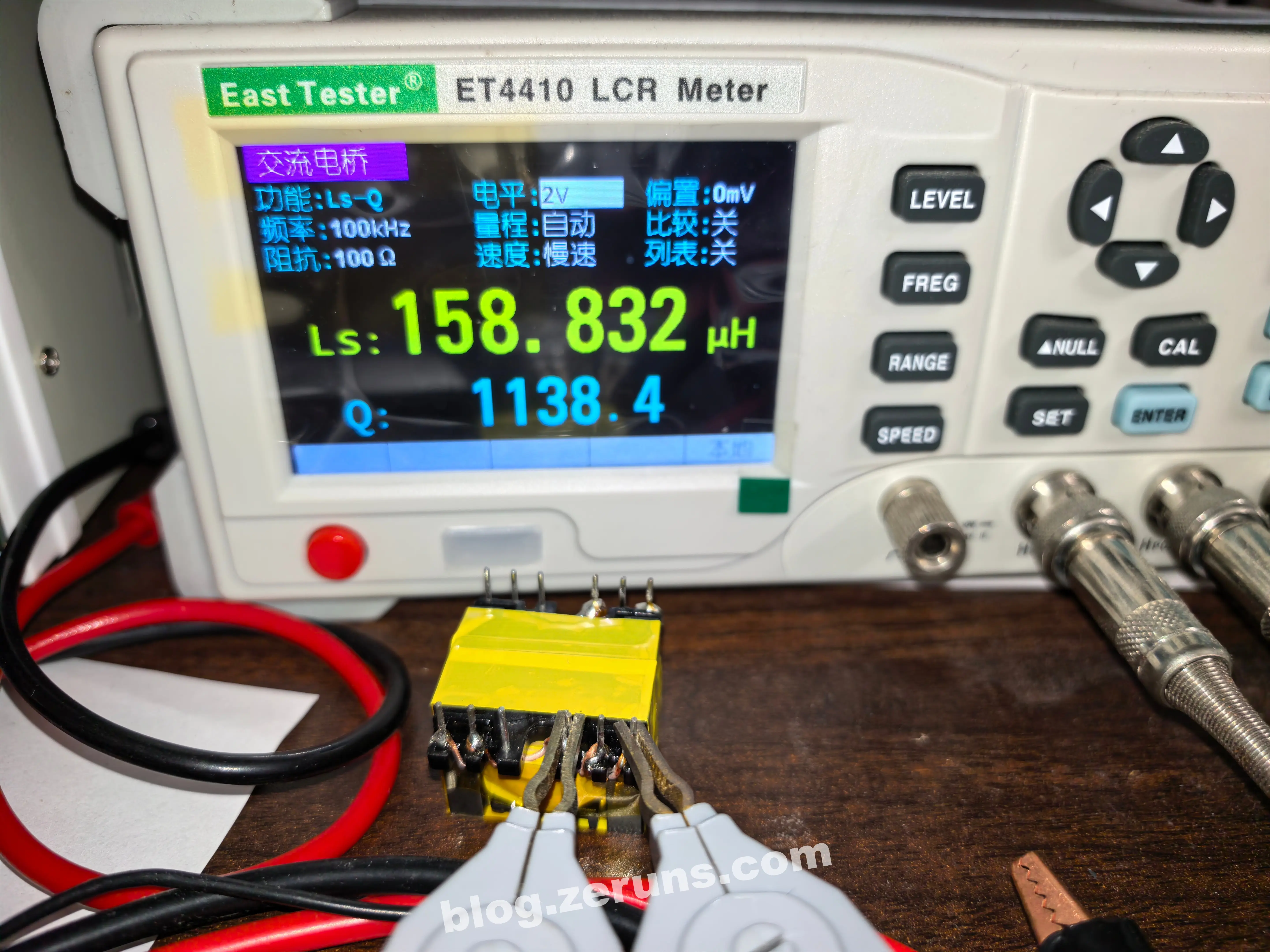
High-frequency transformer:
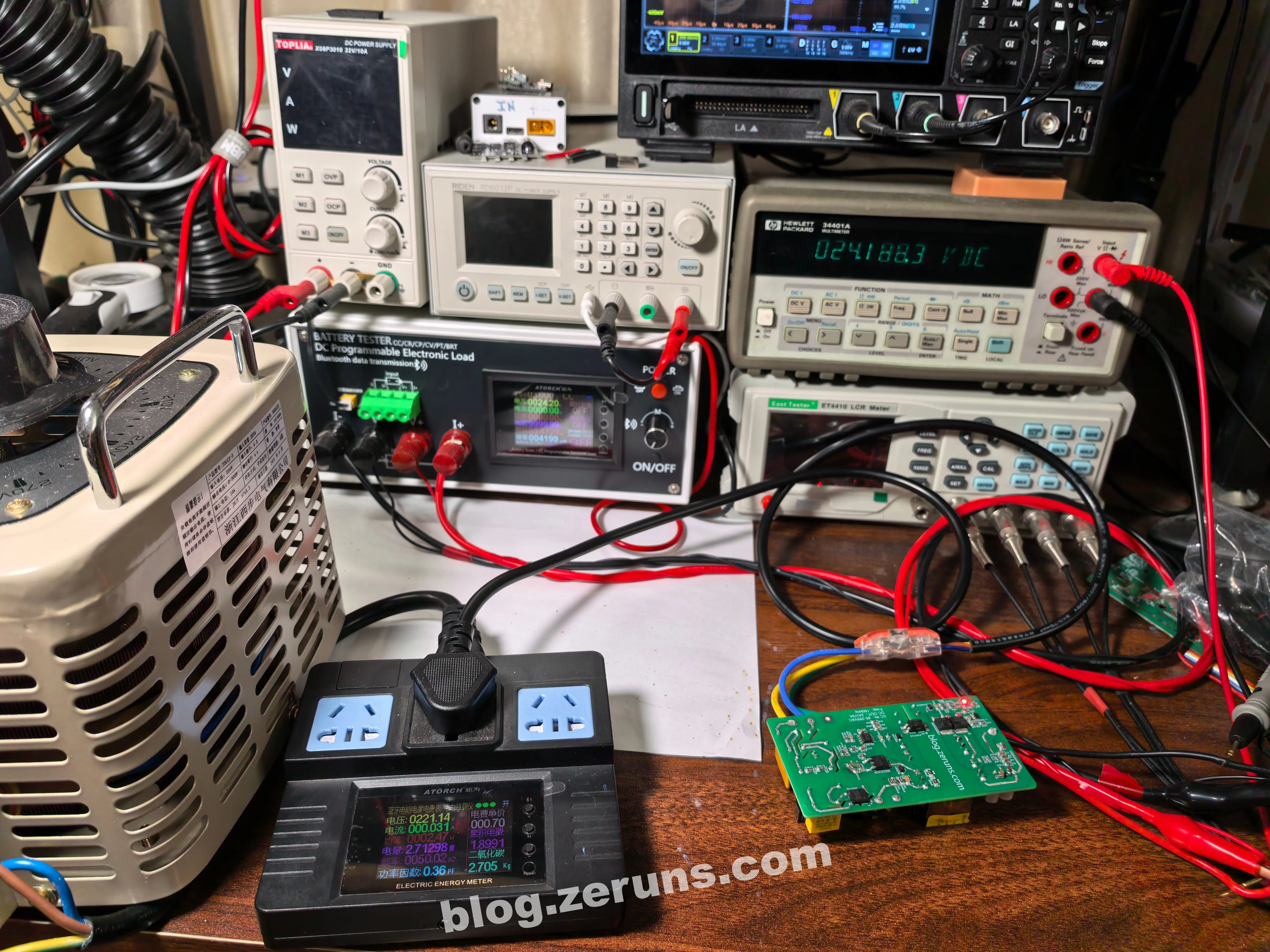
Operational Testing and Performance Measurement
Initial Power-On Test
For the initial power-on test, connect a light bulb in series to prevent blowing a whole set of components in case of a short circuit. The test confirmed normal operation, with an output voltage of 24.1V (the picture below shows the test with a 0.9A load).
The purpose of the series light bulb is: to utilize its current-limiting protection effect. Under normal conditions, the bulb's resistance is low, causing a small voltage drop, so it is dimly lit or off, not affecting the power supply test. If a short circuit occurs inside the power supply, the loop current will surge. The bulb, with its fixed resistance, will drop most of the voltage, limiting the excessive current and preventing the power supply components from burning out due to high current, thus providing protection.
Switching Power Supply Maintenance and Protection Socket: https://s.click.taobao.com/OiMyz3q
You can also test it with a DC input. I tested it with a 60V DC input, and it started up normally and output 24V. However, you need to change the 200kΩ start-up resistor (R24+R16) to a 100kΩ one (short one of them). The original resistance was too high, preventing startup at low voltages.
Conversion Efficiency Test
Test equipment used:
- Jùwéi Power Meter: https://u.jd.com/0gXabte
- Jùwéi Electronic Load: https://s.click.taobao.com/DvbzQ4q
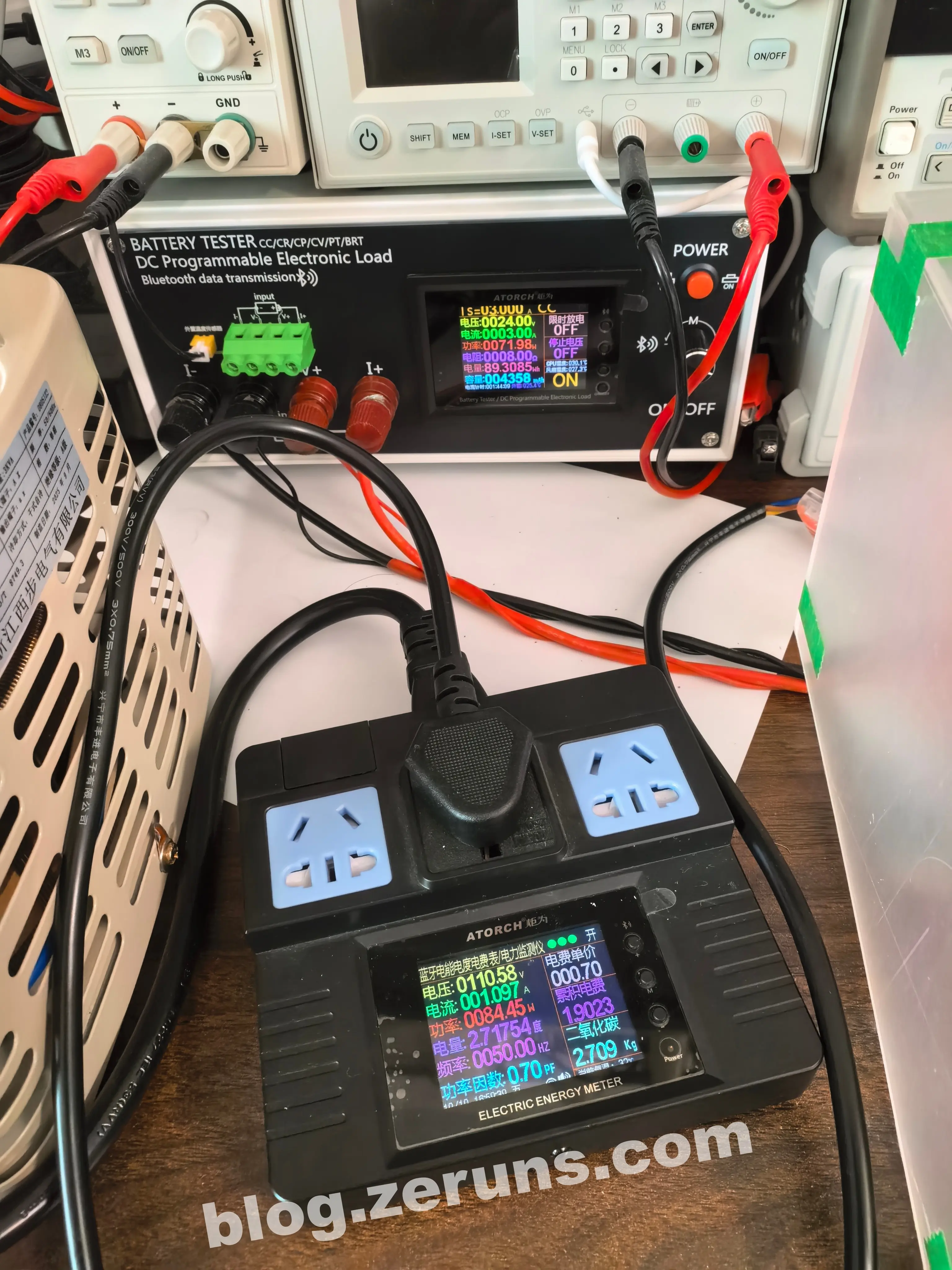
Measured Data:
| Input Voltage (V) | Input Current (A) | Input Apparent Power (W) | Input Active Power (W) | Output Voltage (V) | Output Current (A) | Output Power (W) | Efficiency (%) | Power Factor |
|---|---|---|---|---|---|---|---|---|
| 219.85 | 0.029 | 6.38 | 2.10 | 24.13 | 0.00 | --- | --- | 0.33 |
| 219.83 | 0.251 | 55.18 | 28.69 | 24.10 | 1.00 | 24.10 | 83.99 | 0.52 |
| 219.59 | 0.438 | 96.18 | 55.78 | 24.07 | 2.00 | 48.14 | 86.30 | 0.58 |
| 219.65 | 0.637 | 139.92 | 82.55 | 24.05 | 3.00 | 72.15 | 87.40 | 0.59 |
| 111.55 | 0.036 | 4.02 | 1.81 | 24.13 | 0.00 | --- | --- | 0.45 |
| 111.13 | 0.406 | 45.12 | 28.88 | 24.10 | 1.00 | 24.10 | 83.46 | 0.64 |
| 110.89 | 0.753 | 83.50 | 56.78 | 24.06 | 2.00 | 48.12 | 84.75 | 0.68 |
| 110.58 | 1.097 | 121.31 | 84.91 | 24.00 | 3.00 | 72.00 | 84.79 | 0.70 |
The highest measured efficiency is 87.4%. The lowest no-load power consumption is 1.81W, which is slightly high.
The data above was measured using diode rectification, not synchronous rectification. This is because the on-resistance of the synchronous rectification MOSFET I chose was a bit high, which resulted in slightly lower efficiency. You can replace it with a better MOSFET for testing. The voltage rating should be 200V or higher (a MOSFET with a 150V rating can be considered if you solder a 20Ω resistor and a 2.2nF capacitor for R9 and C8 respectively on the synchronous rectifier side).
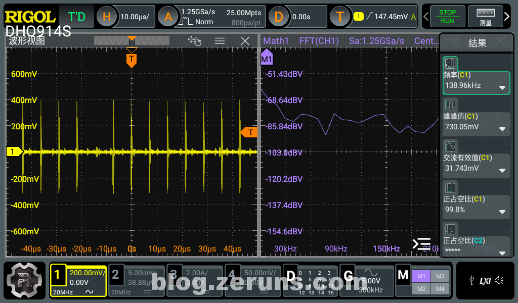
Output Voltage Ripple Test
The oscilloscope used is a Rigol DHO914S: https://blog.zeruns.com/archives/764.html
During testing, the oscilloscope probe was clipped to an output wire approximately 15cm long. A ground spring was not used, nor was the probe connected directly across the output capacitor. Therefore, the measured output voltage ripple may be on the higher side.
No-load ripple, with a peak-to-peak value of around 730mV. The ripple frequency is 138.96kHz, close to the switching frequency.
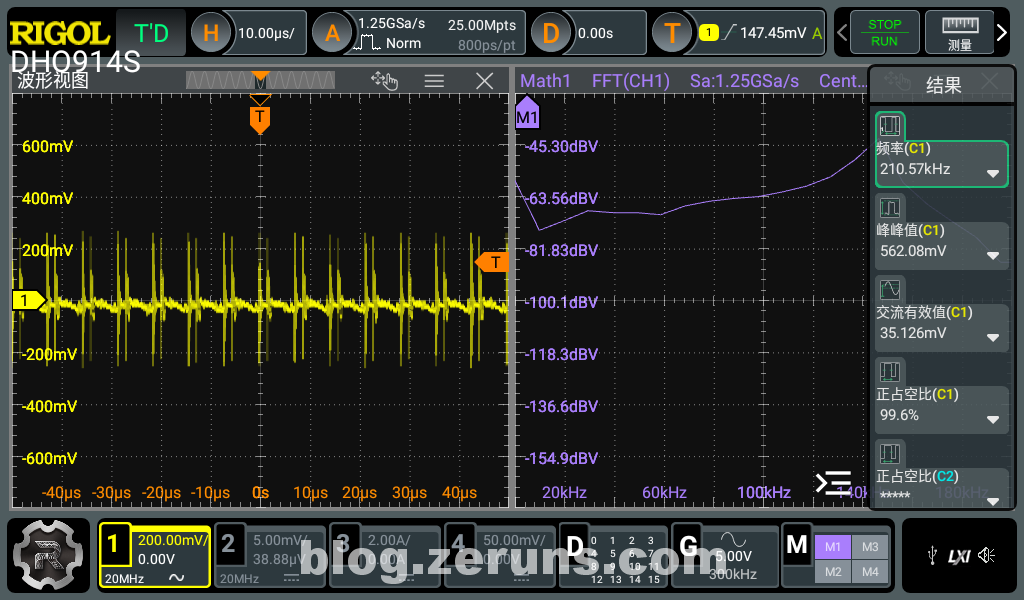
Ripple with a 3A load, with a peak-to-peak value of around 562.08mV.
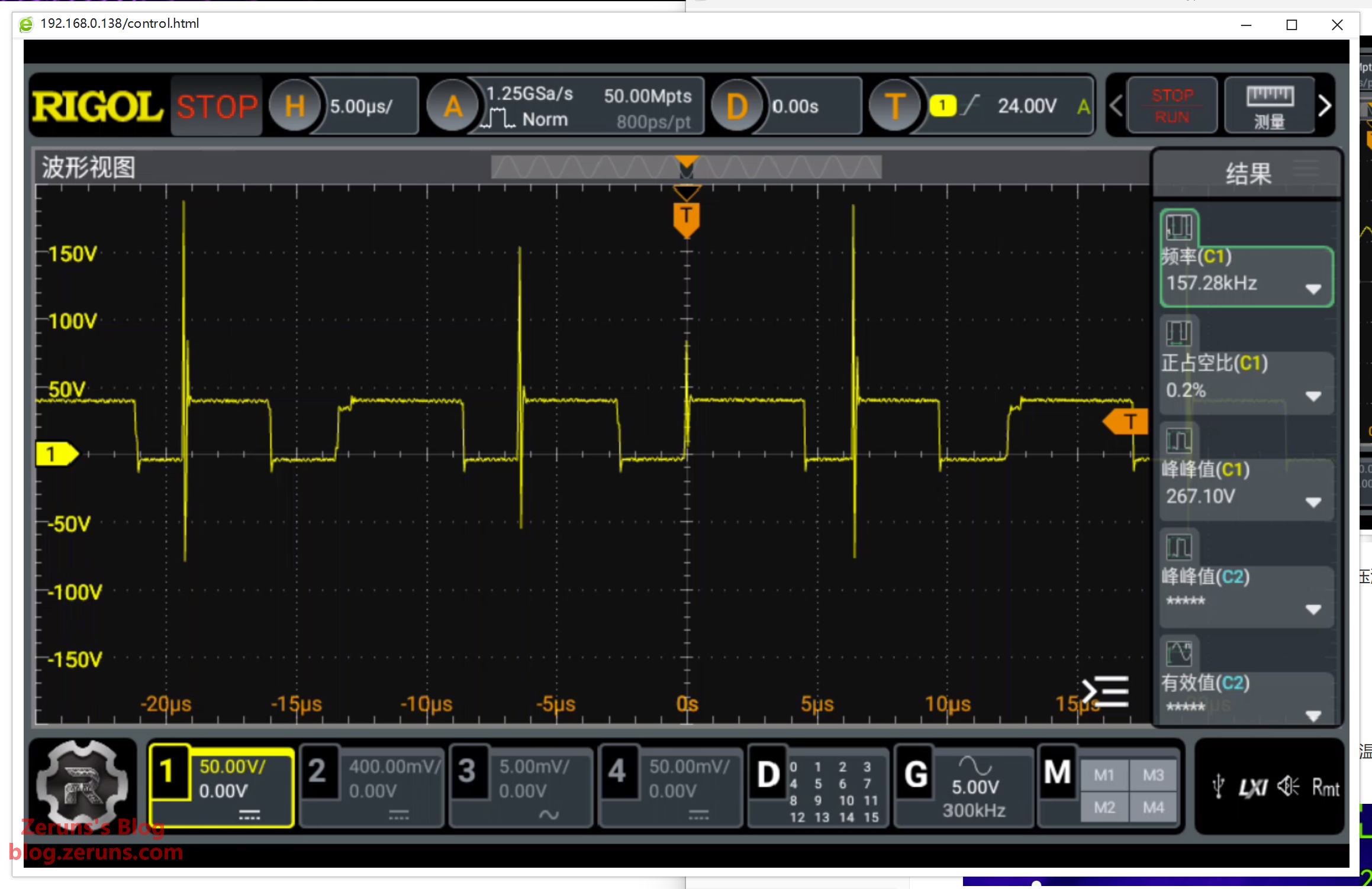
MOSFET Waveforms
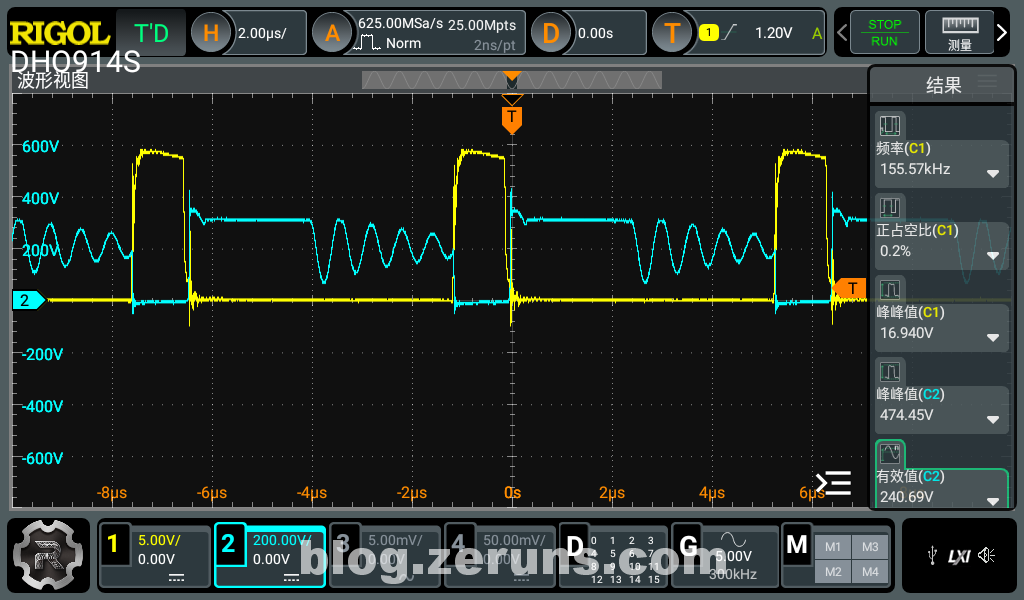
The gate-source (GS) and drain-source (DS) voltage waveforms of the primary-side switching MOSFET with an AC input of 220V and a 1A load at 24V output. The yellow waveform is the voltage between the gate and source, and the blue waveform is the voltage between the drain and source.
It can be seen from the figure that the maximum drain voltage spike when the MOSFET is turned off is approximately 440V (a light bulb is connected in series, and I forgot to switch it to the direct connection mode; therefore, the input voltage of the power supply is probably just over 100V, resulting in a relatively low measured voltage).
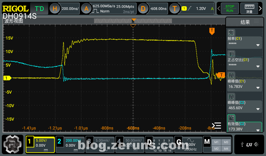
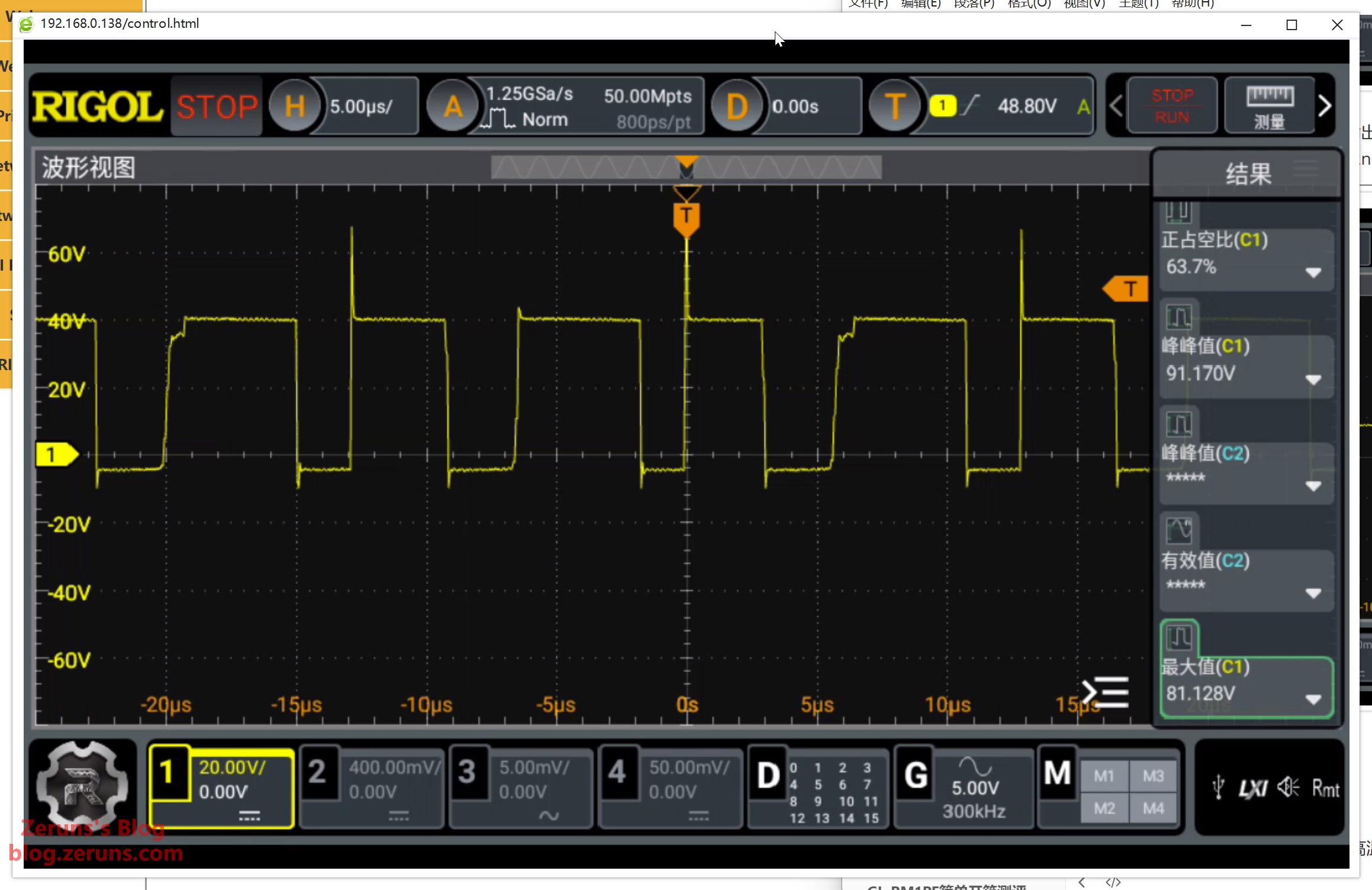
A magnified view of the gate voltage waveform.
Output Rectifier Diode Waveforms
The voltage waveform across the output rectifier diode with a 60V DC input and 24V no-load output is shown below. The voltage spike reaches a maximum of about 56V. (After soldering a 20Ω resistor and a 2.2nF capacitor to R9 and C8 respectively across the diode, the voltage spike drops to 42V).
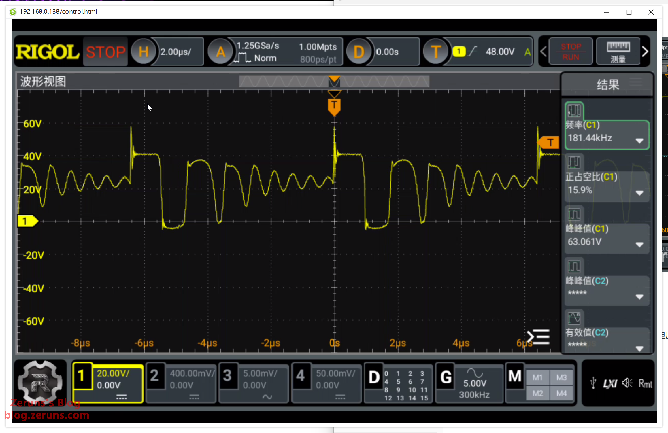
The voltage waveform across the output rectifier diode with a 60V DC input and 24V 1A output is shown below. The voltage spike reaches a maximum of about 190V. (After soldering a 20Ω resistor and a 2.2nF capacitor to R9 and C8 respectively across the diode, the voltage spike drops to 81V).
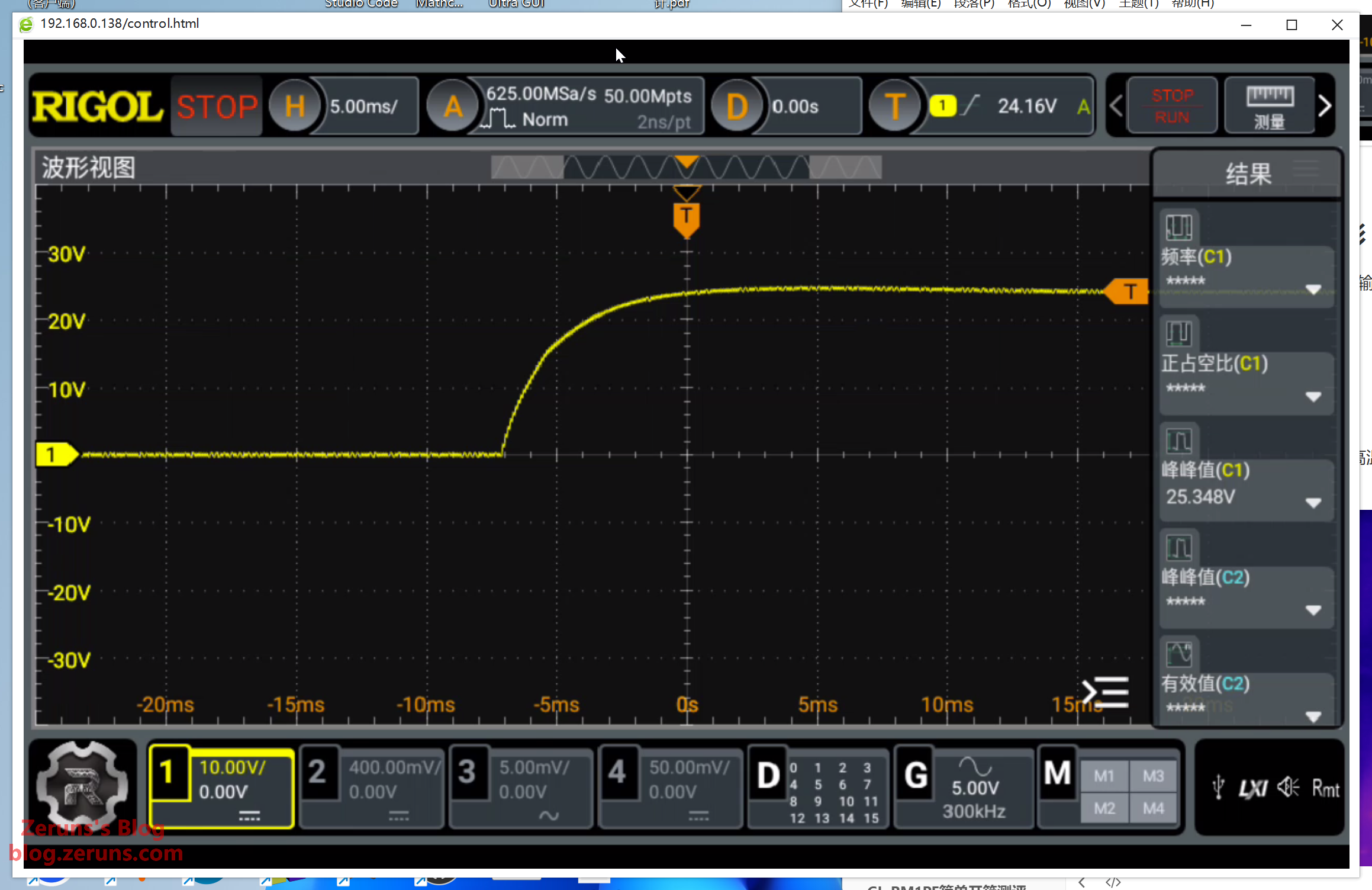
No-Load Startup Output Voltage Waveform
The output voltage waveform with a 60V DC input and 24V no-load output. The time for the voltage to rise from 0V to 24V is 7 milliseconds.
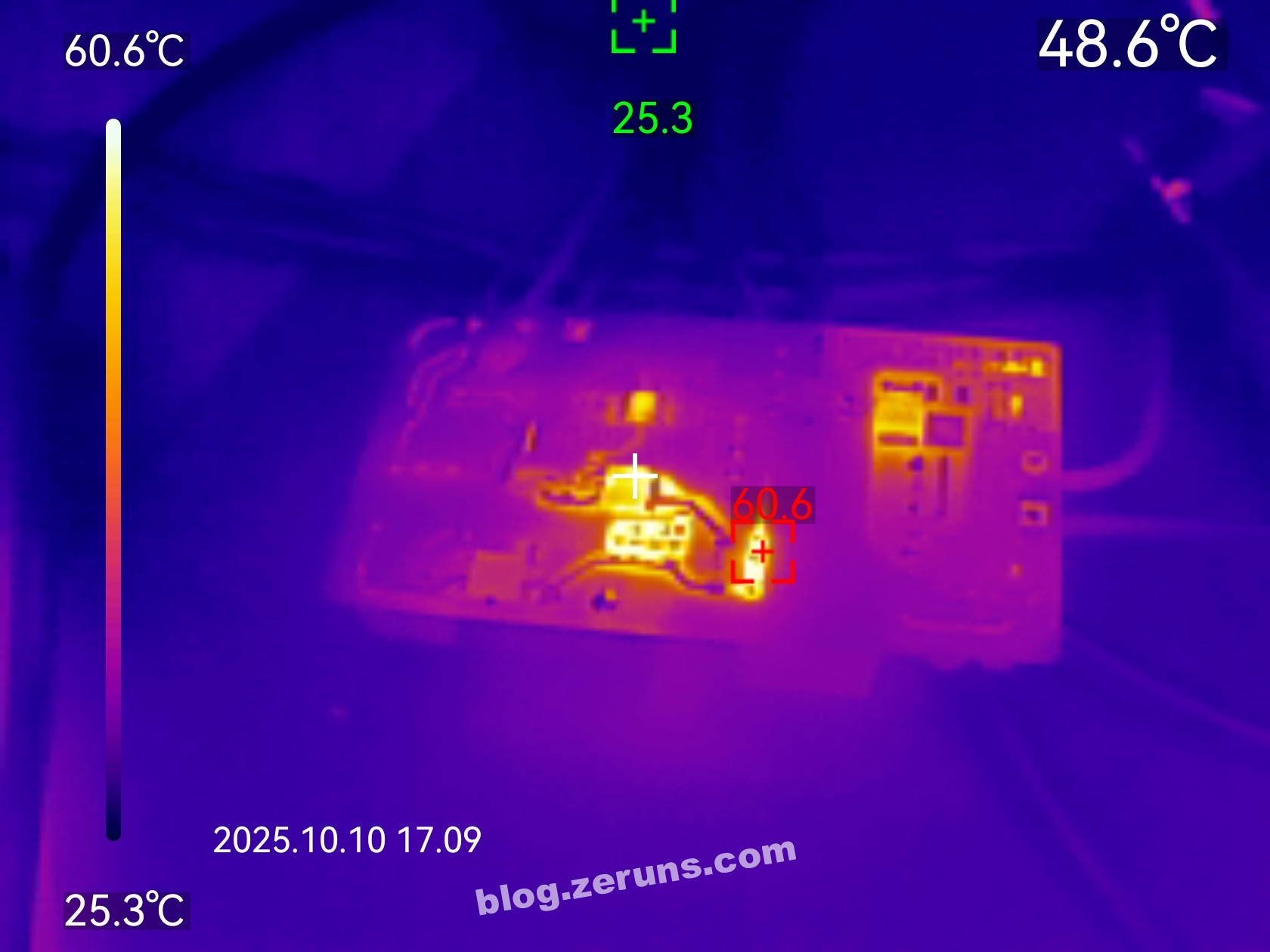
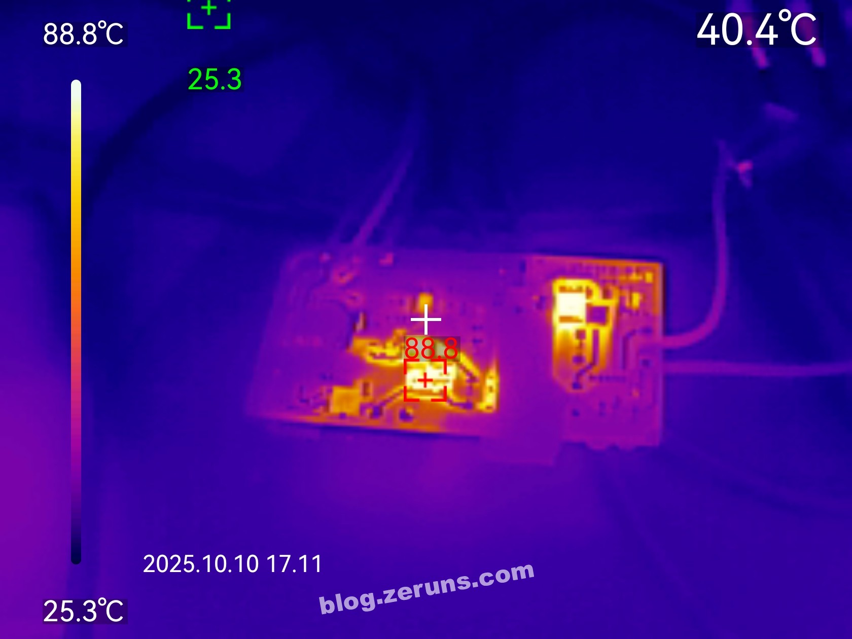
Thermal Performance
Thermal image of the power supply's underside at no load. The hottest spot is on the startup resistor, with a temperature of around 60°C (ambient temperature around 25°C). The primary-side MOSFET is at around 48°C.
Thermal image of the power supply's underside with a 3A load. The hottest spot is on the primary-side MOSFET or the resistor in the RCD snubber circuit, with a temperature exceeding 88°C (ambient temperature around 26°C). The secondary rectifier diode is likely also above 60°C.
The temperature at full load is a bit high. For long-term full-load operation, the primary-side switching transistor will need a heatsink or be potted to transfer heat to the enclosure!
Component Purchase Links
- SMD Resistor and Capacitor Sample Book: https://s.click.taobao.com/ngH2RGq
- PQ Transformer Core and Bobbin: https://s.click.taobao.com/EJtb04q
- UC3842 Chip: https://s.click.taobao.com/7pfvQGq
- PC817A Optocoupler: https://s.click.taobao.com/Le1X04q
- MSB40M Rectifier Bridge: https://s.click.taobao.com/7HqQQGq
- SBDD10200CT Diode: https://s.click.taobao.com/izw104q
- UCC24612-1 Synchronous Rectifier Controller: https://s.click.taobao.com/K1gEQGq
- TL431 Voltage Reference: https://s.click.taobao.com/DPxnz3q
- UU10.5 Common Mode Choke: https://s.click.taobao.com/D1t1z3q
- 5D-11 Thermistor: https://s.click.taobao.com/IsOry3q
- X2 Safety Capacitor: https://s.click.taobao.com/vBeCPGq
- Y Safety Capacitor: https://s.click.taobao.com/sas5PGq
It is recommended to purchase components from LCSC: https://activity.szlcsc.com/invite/D03E5B9CEAAE70A4.html
Clicking the "Order Now" button in the BOM section of the open-source link on LCSC will allow you to import all the required components into your shopping cart with one click.
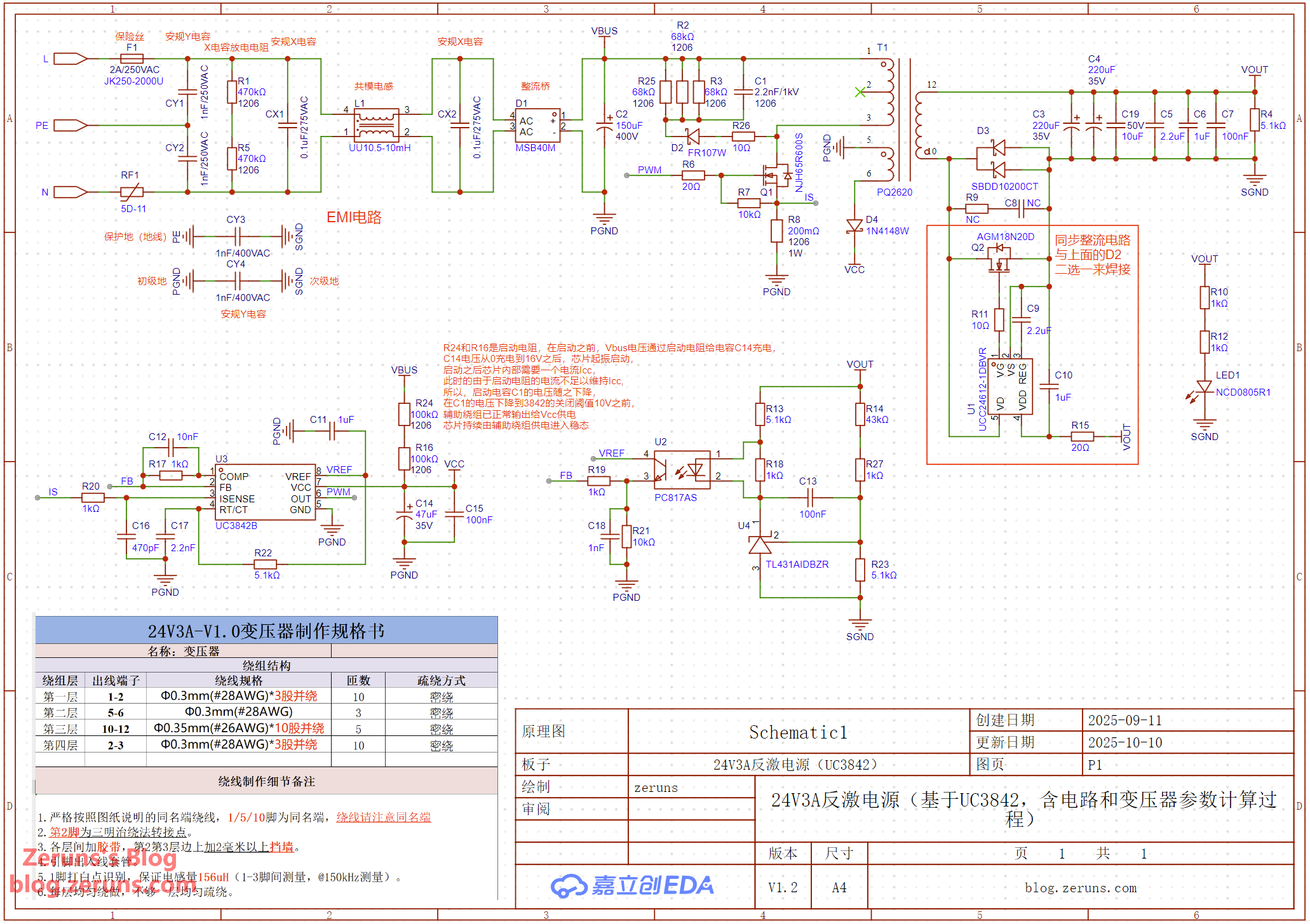
Schematic
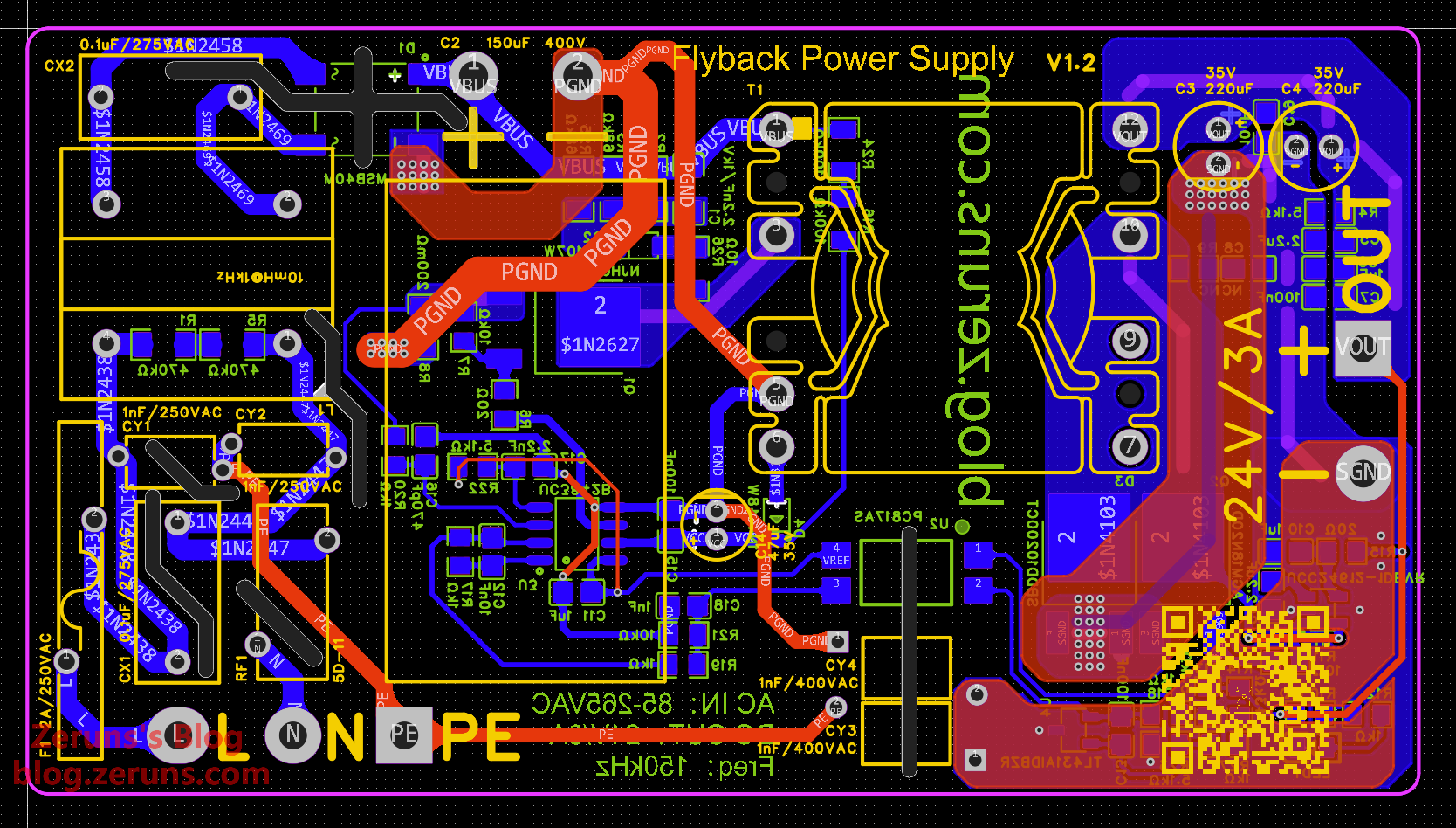
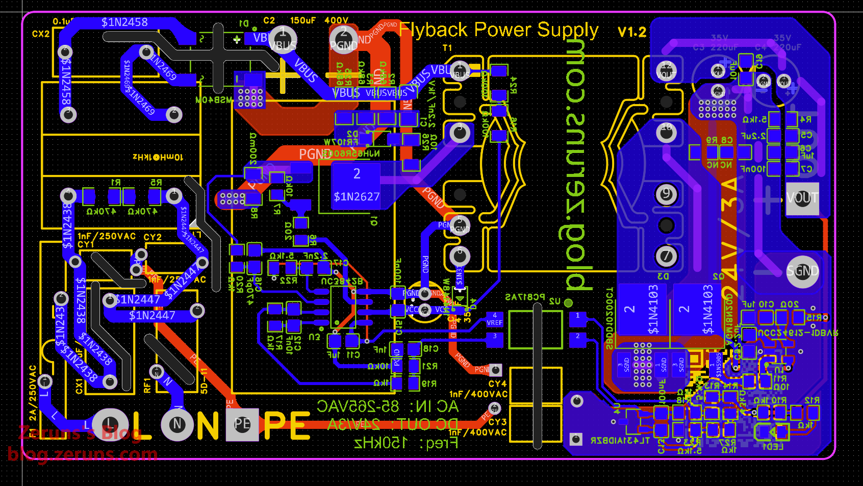
PCB
Top Layer
Bottom Layer
Download Links
The links below contain: JLCEDA project files, schematic PDF, Gerber files for PCB manufacturing, SMPS Design Tool SMPSKit, Flyback Transformer Calculation Sheet (Mathcad), silkscreen diagram, transformer specification sheet, datasheets for various chips, PSIM simulation models, Bode plot Matlab code, and other reference materials and documents. (Some materials were collected from the internet)
- 123 Cloud Drive: https://www.123684.com/s/2Y9Djv-2hTdH
- Baidu Pan: https://pan.baidu.com/s/1767xJthTFWQbxgeZQXM_Hg?pwd=9527 Extraction Code: 9527
If you find this useful, you can support me by donating through the 123 Cloud Drive link above. If you're reading this on WeChat (Official Account: zeruns-gzh), you can also tap the "Like Author" button at the bottom of the article. Thank you.
Recommended Open Source Projects
- An open-source three-phase power collector for easy home energy monitoring: https://blog.zeruns.com/archives/771.html
- Open-source STM32-based synchronous rectification Buck-Boost digital power supply: https://blog.zeruns.com/archives/791.html
- LM25118 Auto Buck-Boost Adjustable DC-DC Power Module: https://blog.zeruns.com/archives/727.html
- Open-source CH32V307-based smart electronic load, from an embedded competition: https://blog.zeruns.com/archives/785.html
- EG1151 High-Power Synchronous Rectification Adjustable Buck-Boost Power Module (supports Type-C PD fast charging input) open-source: https://blog.zeruns.com/archives/794.html
- Open-source 140W+65W Buck-Boost PD3.1 Fast Charging Module (2C+1A ports), IP6557+IP6538, 205W Desktop Charger: https://blog.zeruns.com/archives/801.html
- Open-source Type-C Hub with 4x 10Gbps USB-A ports, a 2.5G network card, and a card reader:https://blog.zeruns.com/archives/868.html
Recommended Reading
- Recommendations for Cost-Effective and Cheap VPS/Cloud Servers: https://blog.zeruns.com/archives/383.html
- Minecraft Server Setup Tutorial: https://blog.zeruns.com/tag/mc/
- Cross-Border E-commerce Independent Website Setup Tutorial, WordPress Foreign Trade Website Guide: https://blog.zeruns.com/archives/889.html
- ZGRL-80 Photography Light Teardown and Circuit Design Analysis: https://blog.zeruns.com/archives/882.html
- Mechrevo Code10AI Laptop (Ultra7-255H) Quick Unboxing Review and Teardown: https://blog.zeruns.com/archives/895.html
- GL-RM1PE Quick Unboxing Review and Teardown, Enabling BMC Remote Management on a Regular PC: https://blog.zeruns.com/archives/900.html


Comment Section