


A simple teardown and analysis of the DJI Mini 2 drone.
A while ago, I noticed that the 5.8GHz wireless image transmission signal of the DJI Mini 2 drone I bought four years ago was extremely weak. After searching online, this phenomenon is suspected to be a faulty 5.8G wireless power amplifier chip, which is said to be a common issue. Since it was out of warranty, I tried to disassemble and replace it myself.
Note: Some chip information interpretations in the article include AI-generated content!
Simple Unboxing and Review of the DJI Mavic Mini 2 Drone: https://blog.zeruns.com/archives/650.html
Other Teardown Articles
- Simple Unboxing, Review and Teardown of GL-RM1PE: https://blog.zeruns.com/archives/900.html
- Teardown and Circuit Design Analysis of ZGRL-80 Photography Light: https://blog.zeruns.com/archives/882.html
- Teardown of ZTE F7015TV3 2.5G ONU: https://blog.zeruns.com/archives/797.html
- Teardown Analysis of Leadise D1500 Uninterruptible Power Supply (UPS): https://blog.zeruns.com/archives/792.html
- Test and Teardown of a 120W Charger for 2.6 Yuan from Douyin Mall: https://blog.zeruns.com/archives/786.html
- Simple Review and Teardown of Apple Mac Mini M4 Mini Host: https://blog.zeruns.com/archives/851.html
Teardown
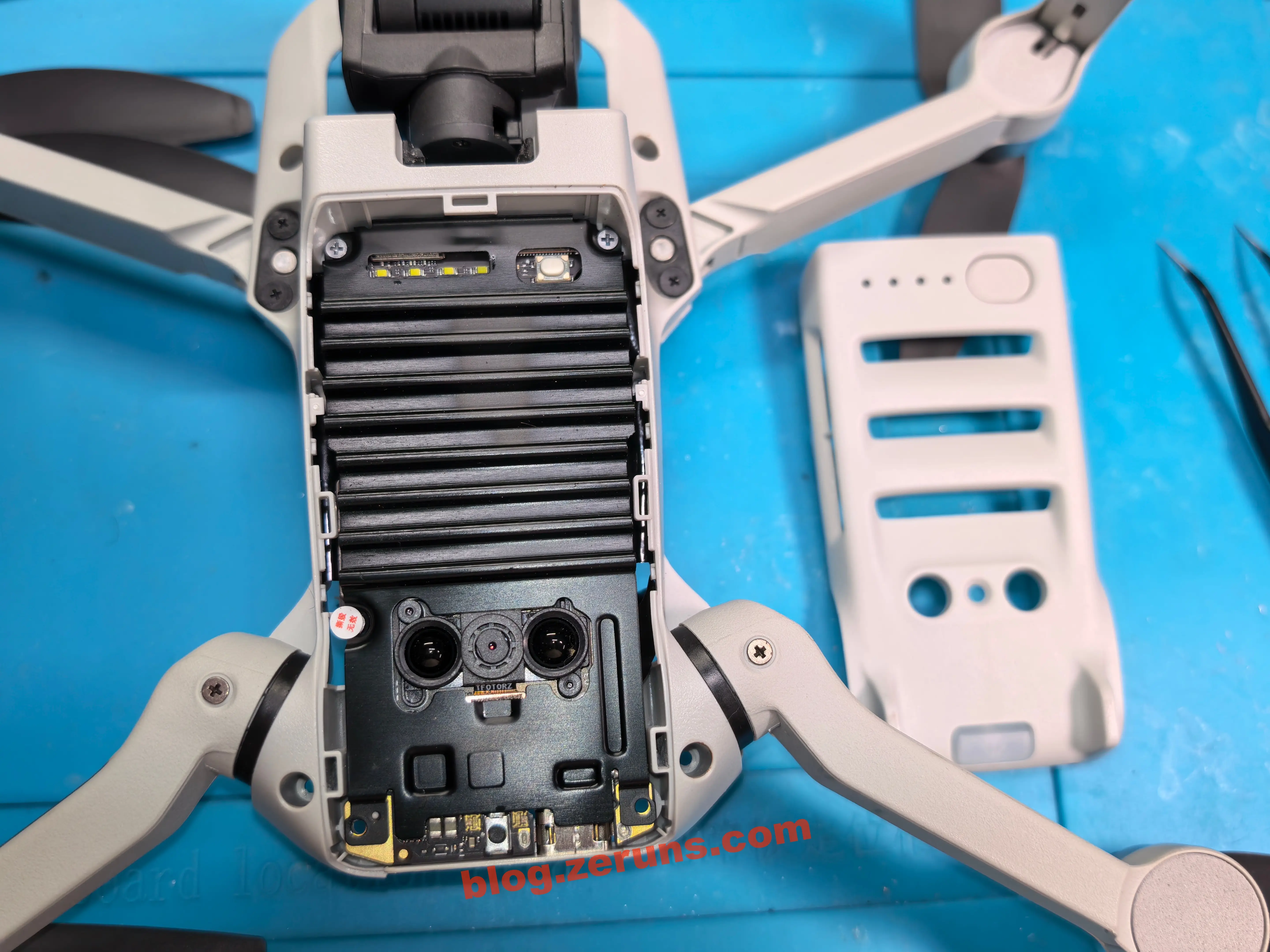
Unscrew the cross screws around the bottom of the drone.
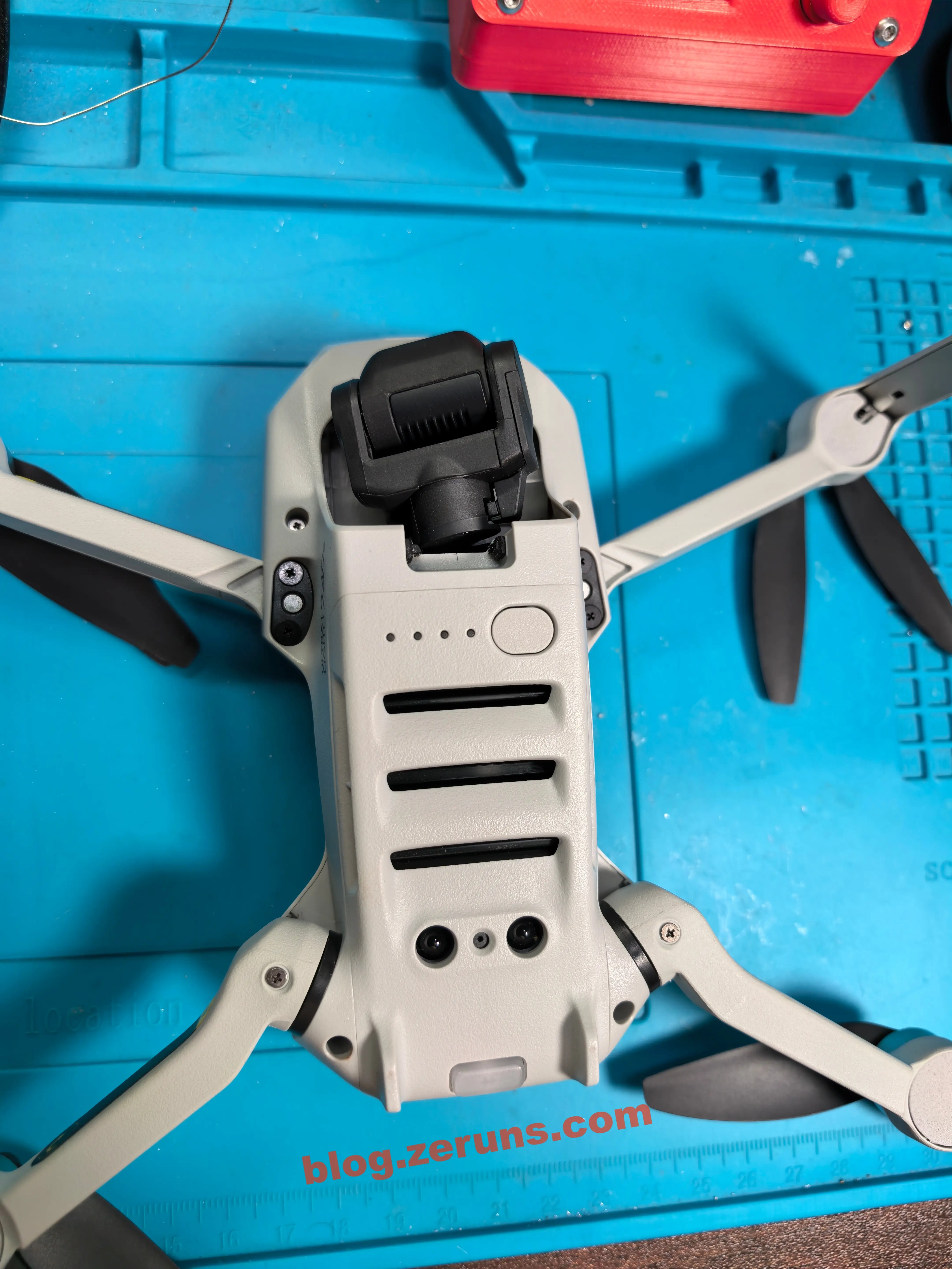
Remove the battery and pry open the shell buckles on both sides inside the battery compartment.
Then you can take off the top cover of the shell. In the middle, you can see the GPS ceramic antenna.
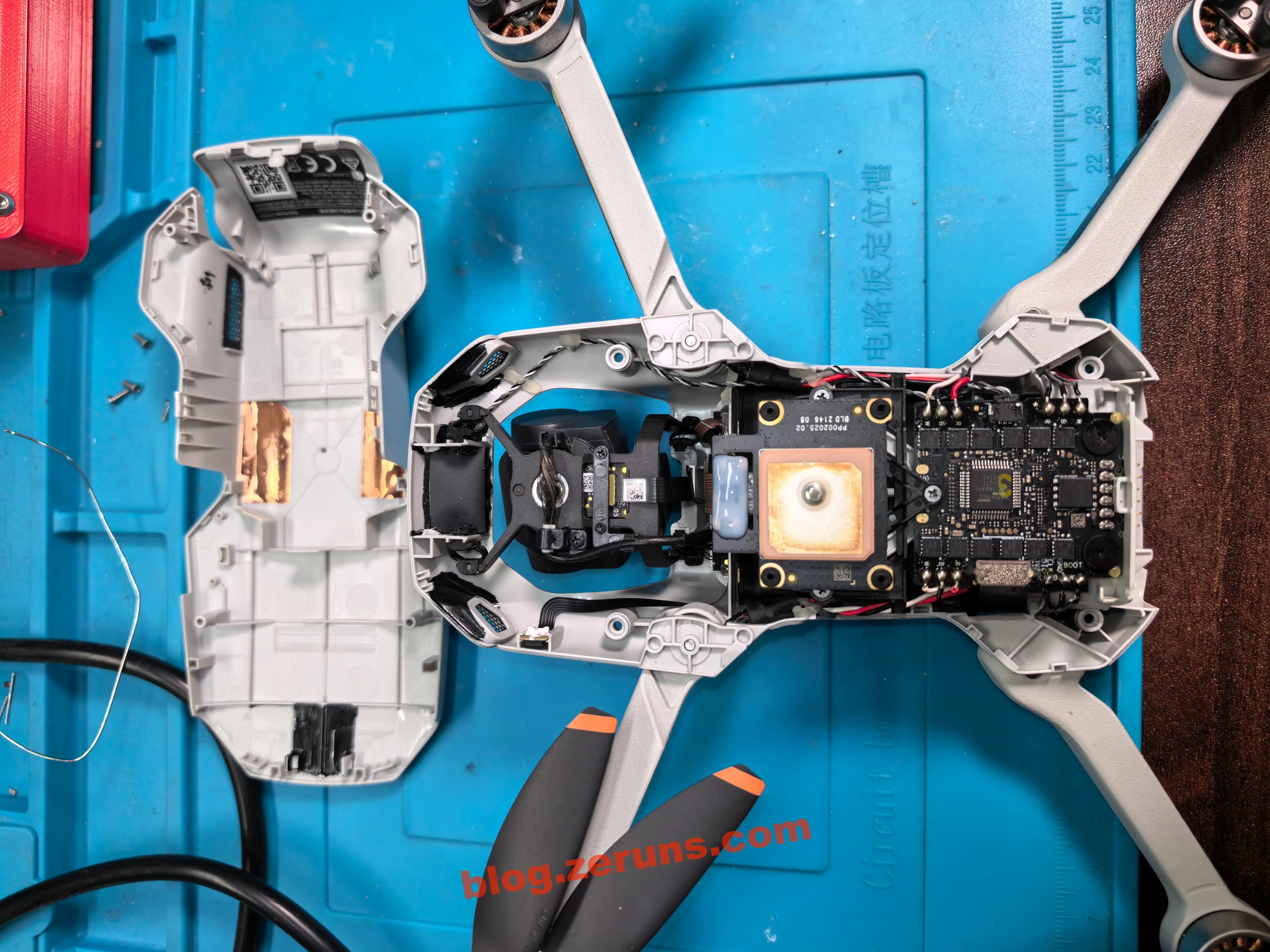
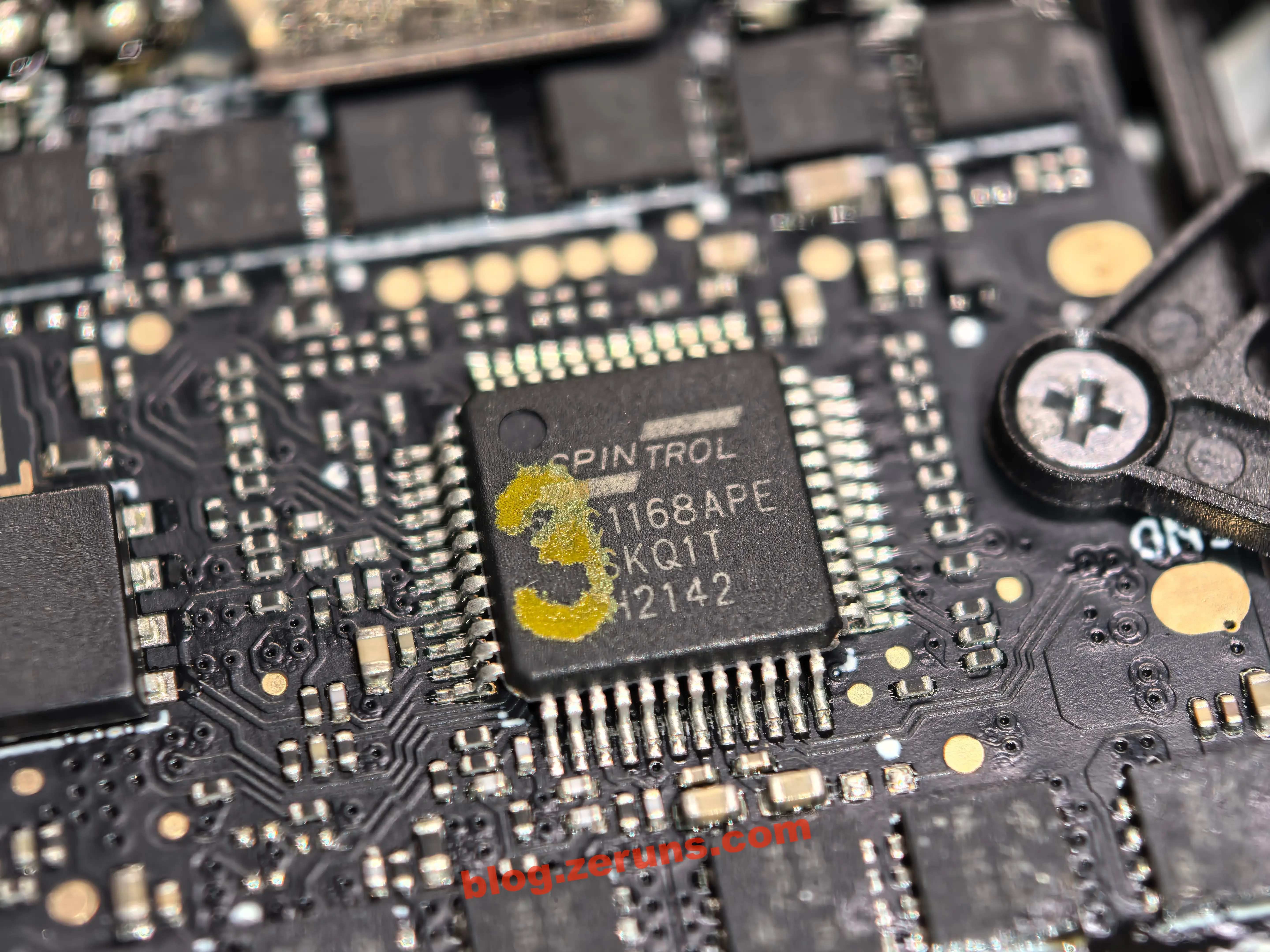
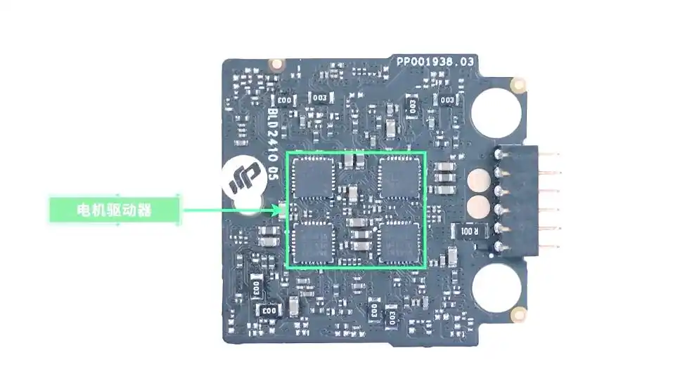
The circuit board under the GPS antenna is the three-phase sensorless BLDC (Brushless DC Motor) driver board. The chip model in the middle of the circuit board is SPC1168APE48, a highly integrated System-on-Chip (SoC) microcontroller from SPINTROL, which is supposed to be used for motor control, regulating the surrounding MOSFETs to drive the motors.
The SPC1168 features a 32-bit high-performance ARM Cortex-M4 core with a maximum software-programmable clock frequency of 200MHz, 64KB SRAM, 128KB embedded FLASH, and abundant enhanced I/O and peripheral resources. It integrates a 14-bit ADC, 3 programmable gain amplifiers, 6 enhanced PWM modules, 3 general-purpose 32-bit timers, and communication interfaces such as UART, I2C, and SPI, making it an ideal platform for motor control applications. Additionally, it adopts two innovative technologies: one is a multi-region security protection technology to improve code security; the other is a flexible IO technology similar to FPGA, which can configure IO as different peripherals to support various application requirements, but with higher cost-effectiveness.
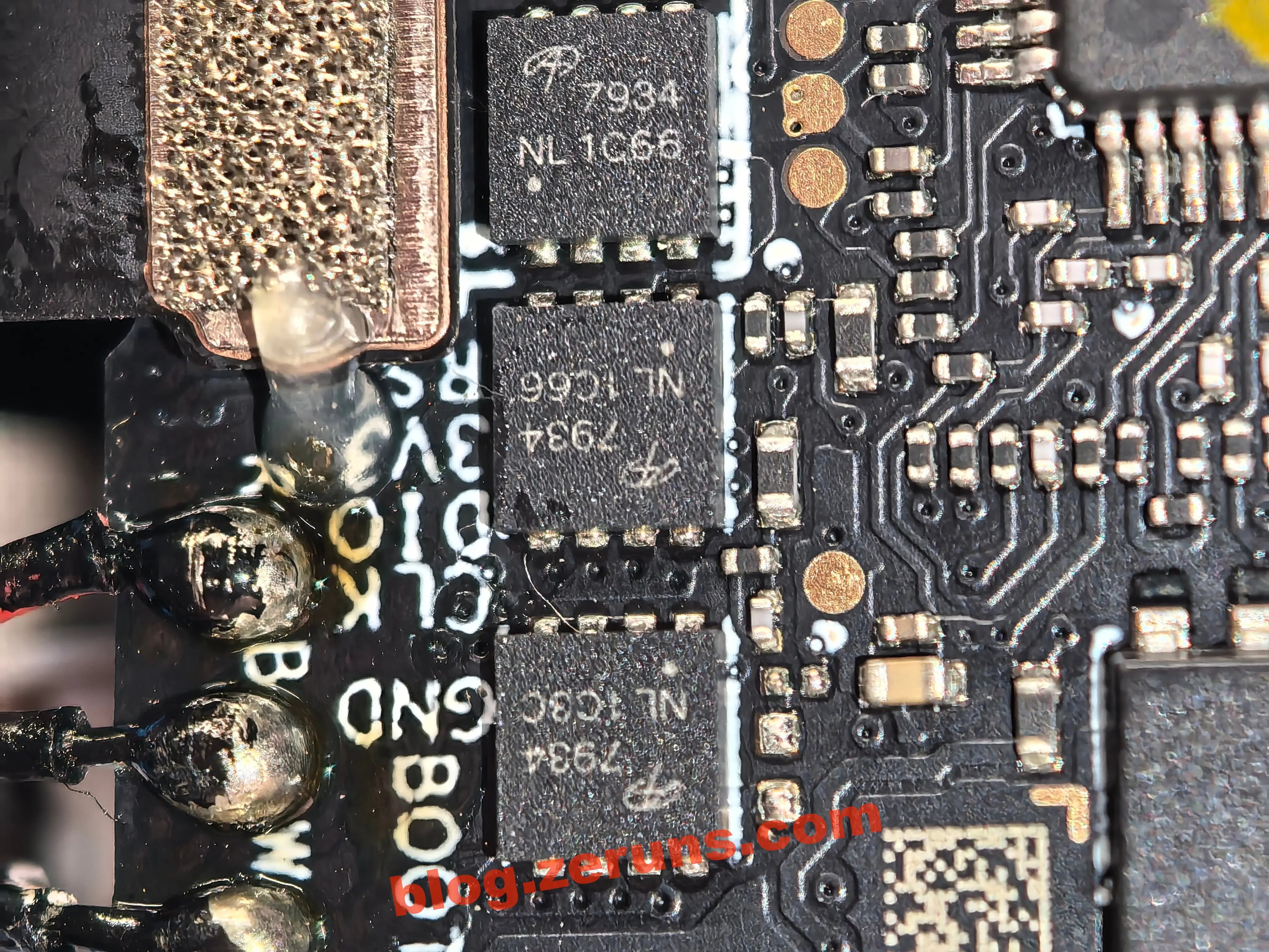
There are 4 groups of MOSFET chips (3 chips per group) around the motor driver board, corresponding to the motors of the four rotors. The MOSFET model is AON7934, a dual N-channel MOSFET from Alpha and Omega Semiconductor Limited (AOS), with two NMOS in a single chip forming a half-bridge.
Core Chip Parameters:
- Electrical Performance:
- Drain-Source Voltage (Vds): 30V
- Continuous Drain Current (Id): 16A/18A (different channels)
- On-Resistance (Rds (on)): Minimum 10.2mΩ @ 16A, 10V
- Input Capacitance (Ciss): 485pF
- Packaging and Reliability: Adopts DFN-8 (3x3) package, supports a wide operating temperature range of -55℃~150℃, meeting the reliability requirements of drones in complex outdoor environments.
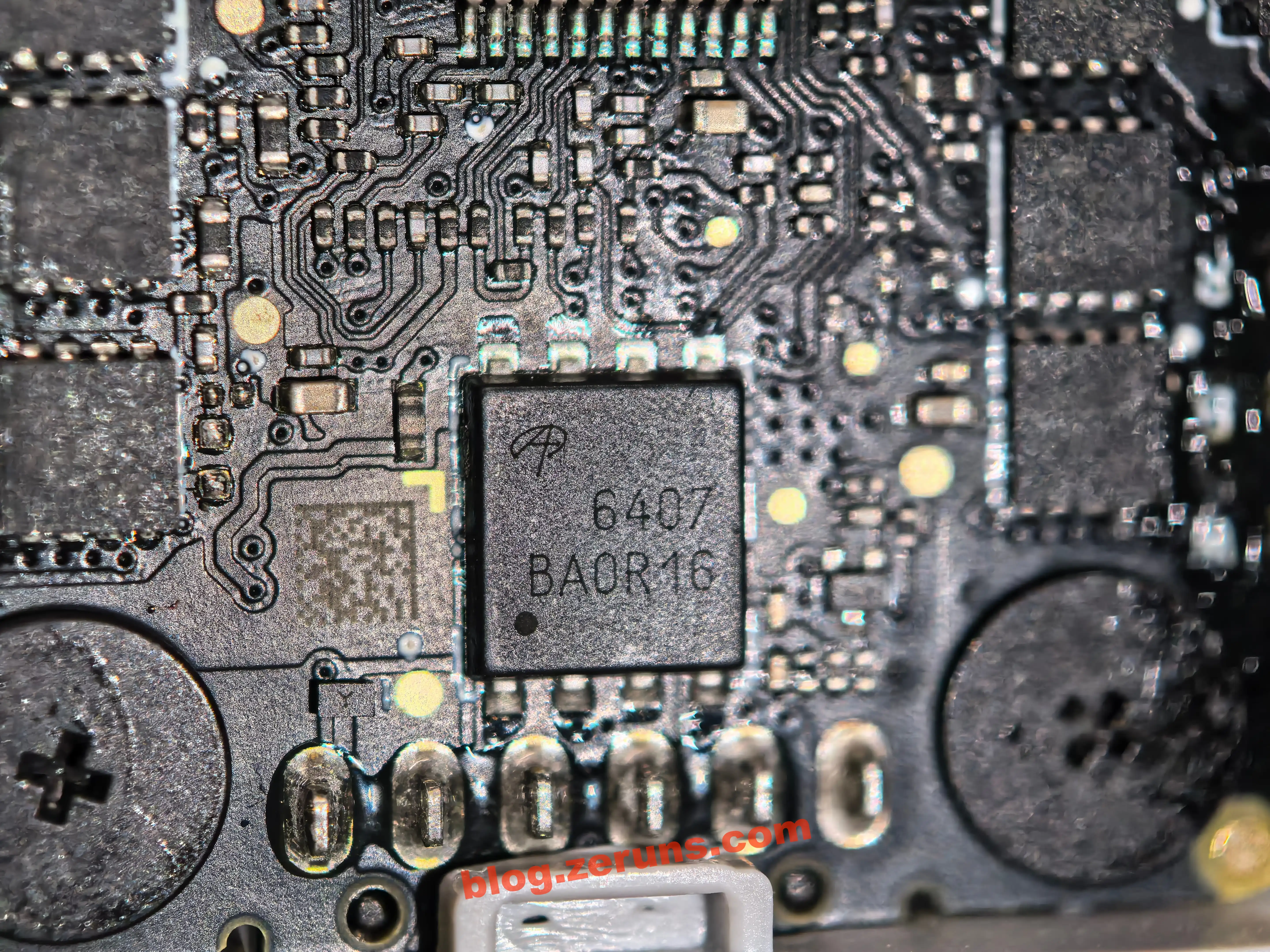
The chip above the battery interface is model AON6407, a P-channel power MOSFET from AOS.
Key Parameters and Characteristics:
- Electrical Performance: Drain-Source Voltage (Vds) -30V, Continuous Drain Current (Id) -85A, On-Resistance (Rds (on)) 4.5mΩ
- Packaging Design: Adopts PDFN-8 (5.8x4.9) package
Function Analysis:
As the power switch tube of the battery power supply circuit, the AON6407 chip undertakes the following key functions above the battery interface:
- Power On/Off Control: Responsible for switching the power transmission between the battery and the drone's main circuit, realizing precise control of power supply during startup and power cutoff during shutdown.
- Efficient Power Transmission: With low on-resistance (4.5mΩ), it reduces power loss during battery power supply, improves power utilization efficiency, and indirectly extends the drone's battery life.
- Circuit Safety Protection: In abnormal working conditions such as overcurrent and overvoltage, it can quickly turn off the circuit to prevent damage to the battery or backend system due to overload, ensuring the reliability of the power supply system.
In short, it is a "power gate" between the battery and the drone's core circuit, which not only ensures efficient power transmission but also builds a safety barrier for the power supply system.
On the back of the motor driver board, there are 4 MP6530 chips from MPS (Monolithic Power Systems), a gate driver IC specifically designed for three-phase brushless DC motor drivers. It can drive 3 half-bridges composed of 6 N-channel power MOSFETs and handle voltages up to 60V.
Unscrew the two cross screws under the battery compartment to remove the bottom cover of the drone.
First, you can see a large black aluminum alloy heatsink, with a downward-facing camera and an infrared ranging module underneath.
After removing the heatsink, the shield and some chips are coated with blue thermal grease.
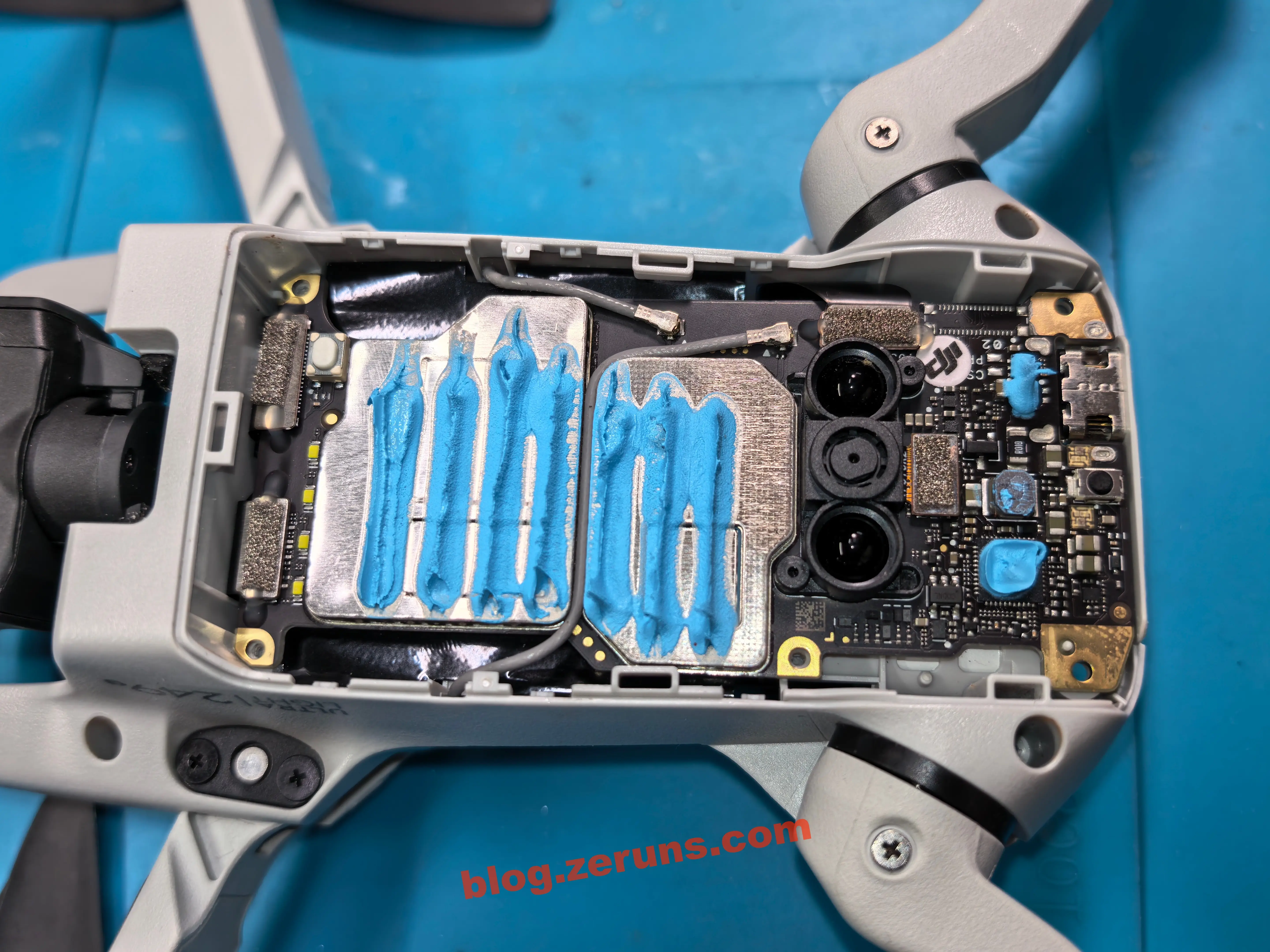
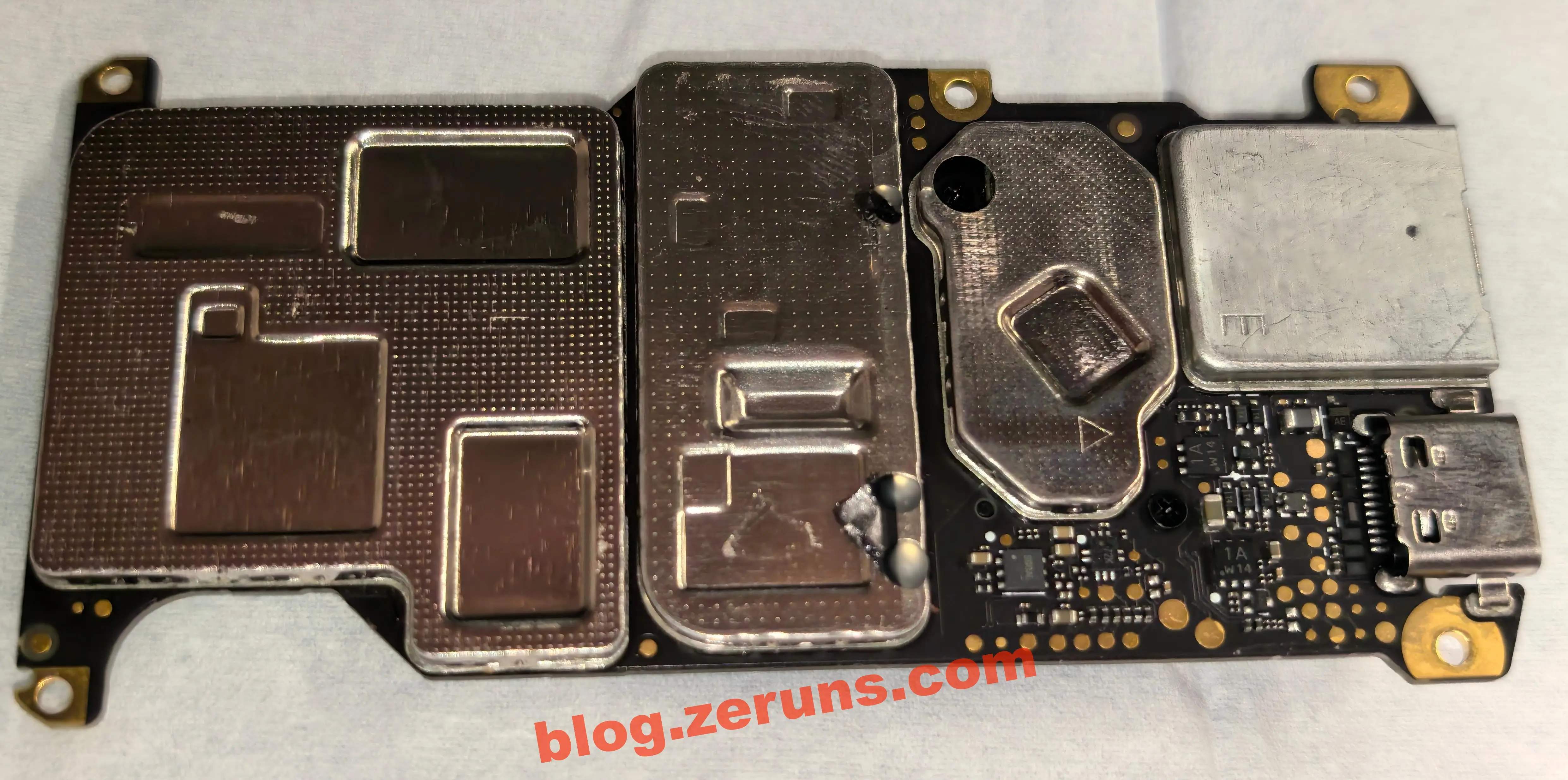
Remove the main board mentioned earlier; the back of the main board houses the Type-C charging port and TF card slot.
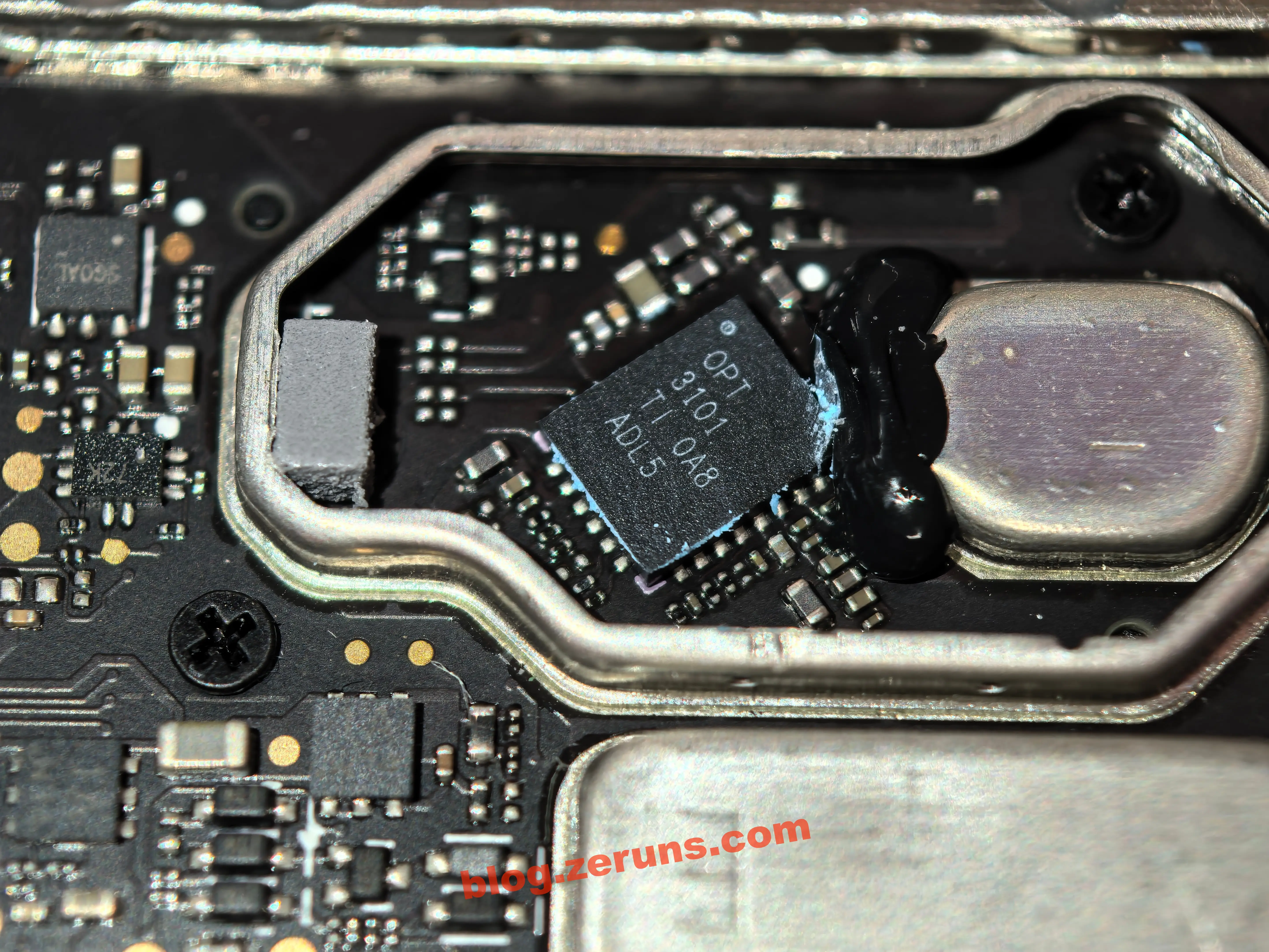
Remove the shield under the TF card slot (the other side of the circuit board at this position is the downward-facing camera module), and there is an OPT3101 chip from Texas Instruments (TI) inside.
Core Attributes and Functions:
- Technology Type: Long-distance proximity and distance sensor analog front-end (AFE) based on Time of Flight (ToF) principle.
- Performance Highlights:
- Ranging Range: Unambiguous within 15 meters, supports 16-bit distance output with a resolution of 3 millimeters;
- Environmental Adaptability: Excellent ambient light suppression capability, can work under full sunlight of 130klx;
- Integration: Built-in ADC, timing sequencer, digital processing engine, and illumination driver, supporting 3 transmitter channels.
Role in the Device:
As the core ToF sensing component, it is mainly used to realize:
- Precise Ranging: Provide real-time distance measurement for drones and other devices to assist flight control and obstacle avoidance decisions;
- Environmental Perception: Identify the distance and direction of surrounding obstacles through multi-area sensing, improving the intelligent interaction and safety performance of the device;
- Anti-Interference Operation: Unaffected by object reflectivity, it can stably output depth data in complex lighting environments.
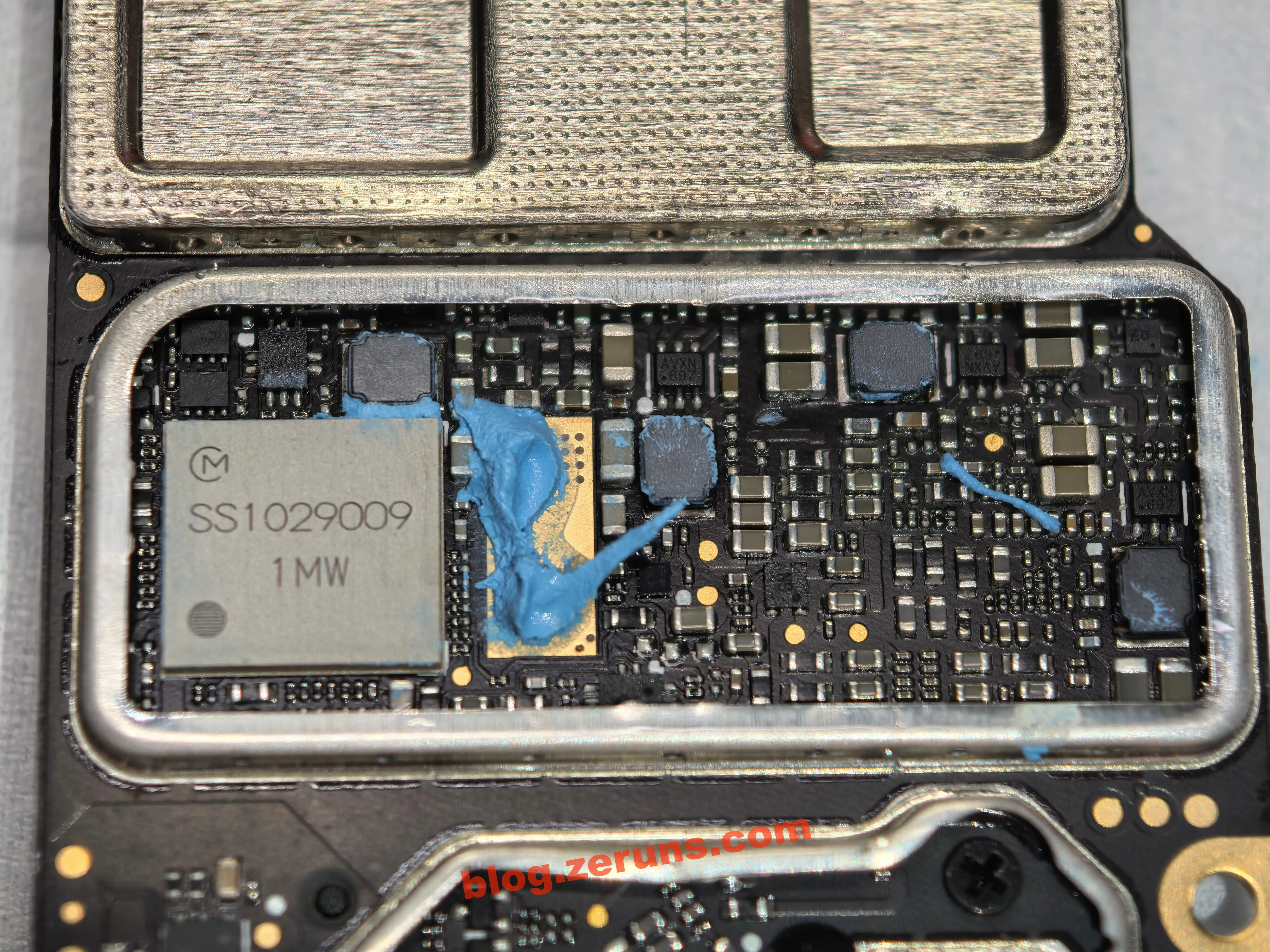
Inside the middle shield, there is a chip model SS1029009 from muRata, which is suspected to be responsible for the modulation and demodulation of the drone's image transmission signal.
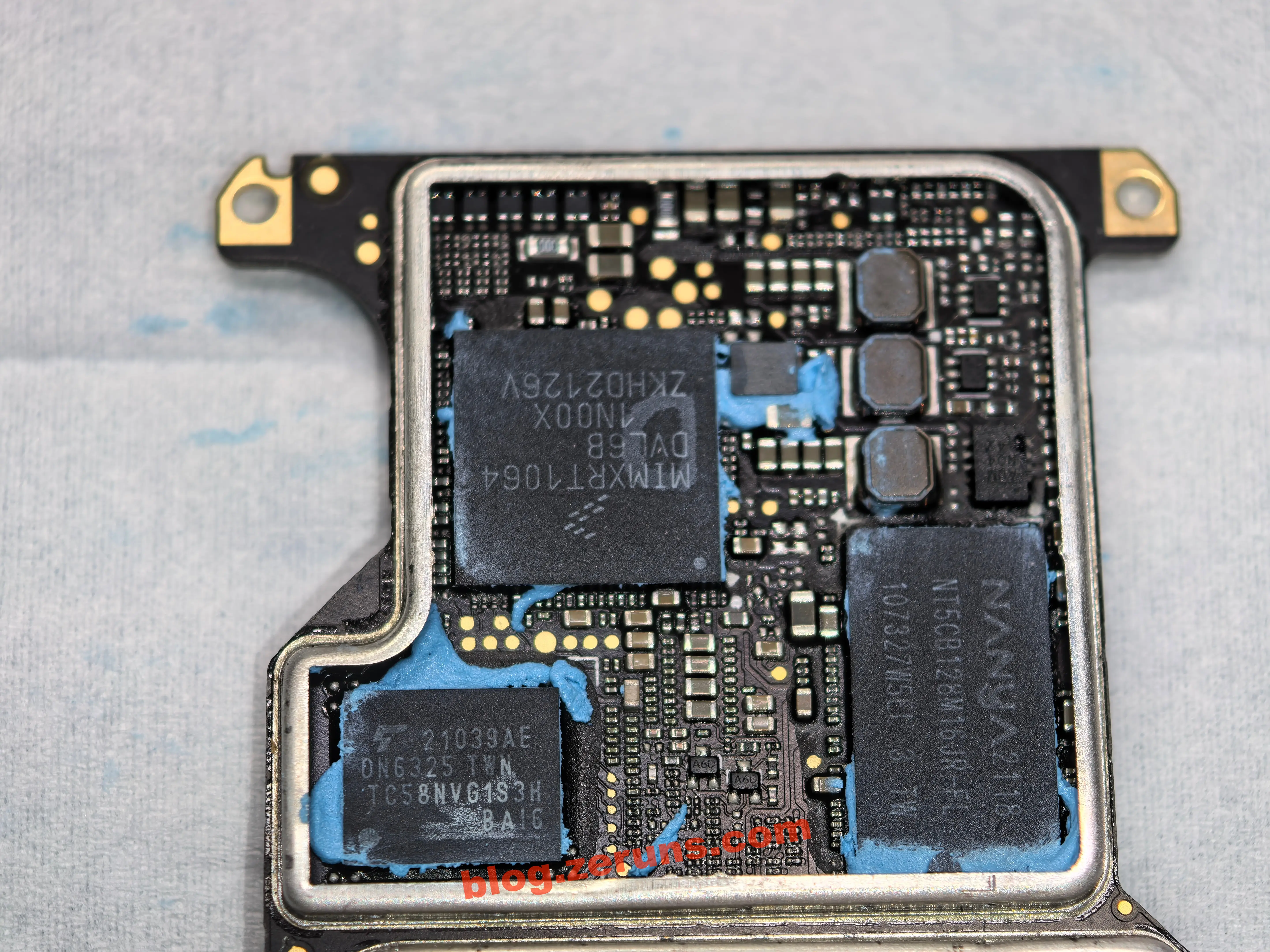
Inside the largest shield, there are three large chips: MIMXRT1064, TC58NVG1S3H, and NT5CB128M16JR-FL.
1. i.MX RT1064 (MIMXRT1064)
- Brand and Positioning: A high-performance crossover processor from NXP, belonging to the i.MX RT series.
- Core Parameters:
- Core: Cortex-M7, with a maximum frequency of 600MHz.
- Storage: Supports external DDR and Flash expansion, with high-speed data processing capabilities.
- Function Role: As the main control chip of the DJI Mini 2, it is responsible for core tasks such as flight control, sensor data fusion, and image preprocessing, serving as the "brain" of the drone.
2. TC58NVG1S3H (Toshiba Flash Chip)
- Brand and Positioning: An SLC NAND flash chip from Toshiba.
- Core Parameters:
- Capacity: 2Gbit (256MByte), an industrial-grade storage device.
- Characteristics: Supports high-speed reading and writing, with power-off data protection function.
- Function Role: Used to store key data such as the drone's firmware program, flight logs, and calibration parameters, ensuring the stability of system startup and function configuration.
3. NT5CB128M16JR-FL (Nanya DDR Memory)
- Brand and Positioning: A DDR3 memory chip from Nanya.
- Core Parameters:
- Capacity: 128M×16bit (2Gbit=256MByte), operating voltage 1.5V.
- Data Rate: Up to 2133 MT/s (equivalent to DDR3-2133), corresponding to a clock frequency of 1066 MHz.
- Performance: Supports high-speed data throughput to meet the high bandwidth requirements of the main control chip.
- Function Role: As running memory, it provides data cache space for the i.MX RT1064, ensuring the smooth operation of tasks such as flight control algorithms and real-time image processing.
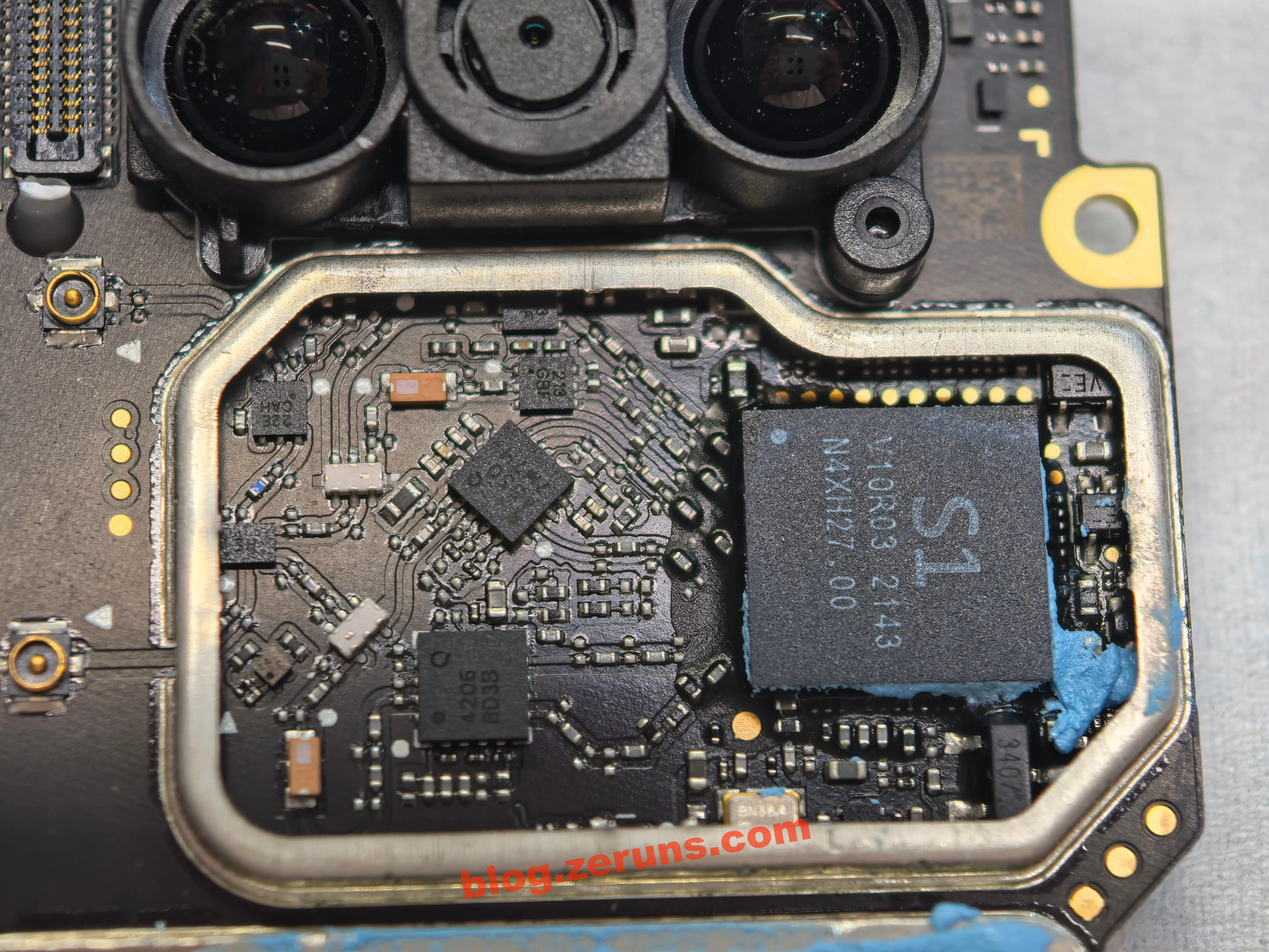
Inside the shield under the downward-facing camera module, there are three main chips: S1 V10R03, 4205, and 4550.
1. S1 V10R03 Chip
- Type: Customized image transmission communication chip (belonging to the S1 series of DJI's OcuSync system, codenamed "Sparrow 1").
- Function: As the core of the drone's image transmission system, it is responsible for modulation, demodulation, data transmission, and encryption of wireless signals, and is a key component for achieving low-latency and high-stability image transmission. It only handles the RF communication part, while tasks such as video encoding are completed by other chips in coordination. Therefore, in entry-level models such as the Mini series, it is more like a "modem".
- Parameter Characteristics: Supports a maximum bandwidth of 20MHz, adopts a customized architecture, optimized specifically for the wireless link of DJI drones, and is only used in DJI ecosystem products, making it one of its technical "moats".
2. 4205 Chip
- Type: 2.4GHz RF power amplifier (speculated to be a chip of the same series as QPF4206, with simplified marking on the silkscreen).
- Function: Amplifies wireless signals in the 2.4GHz band, improving the image transmission distance and anti-interference ability in this band. The 2.4GHz band of the DJI Mini 2 is used for long-distance communication (such as long-distance transmission in open environments), and this chip is crucial for ensuring the performance of this band.
- Parameter Characteristics: Works in the 2.4GHz band, has efficient power amplification capability, can increase the transmit signal strength to the upper limit specified by regulations, and at the same time reduce power consumption to adapt to the battery life requirements of the drone.
3. 4550 Chip
- Type: 5.8GHz RF power amplifier (model QPF4550).
- Function: Amplifies wireless signals in the 5.8GHz band. This band has a wider bandwidth, which is suitable for transmitting high-definition video, but has weak penetration. This chip is responsible for enhancing the transmit power of 5.8GHz signals, ensuring the stability of high-definition image transmission of the Mini 2 in short-distance and low-interference environments (such as low-latency transmission during urban close-up shooting).
- Parameter Characteristics: Optimized specifically for the 5.8GHz band, with high power efficiency, it can maintain signal quality during high-bandwidth transmission, and is one of the core hardware for achieving the "low-latency image transmission" of the Mini 2.
These three chips work together to build the wireless communication system of the DJI Mini 2: S1 is responsible for "encoding and transmission management" of signals, while 4205 and 4550 respectively enhance the signal strength of the 2.4GHz and 5.8GHz bands, ultimately achieving a long-distance and low-latency image transmission experience.
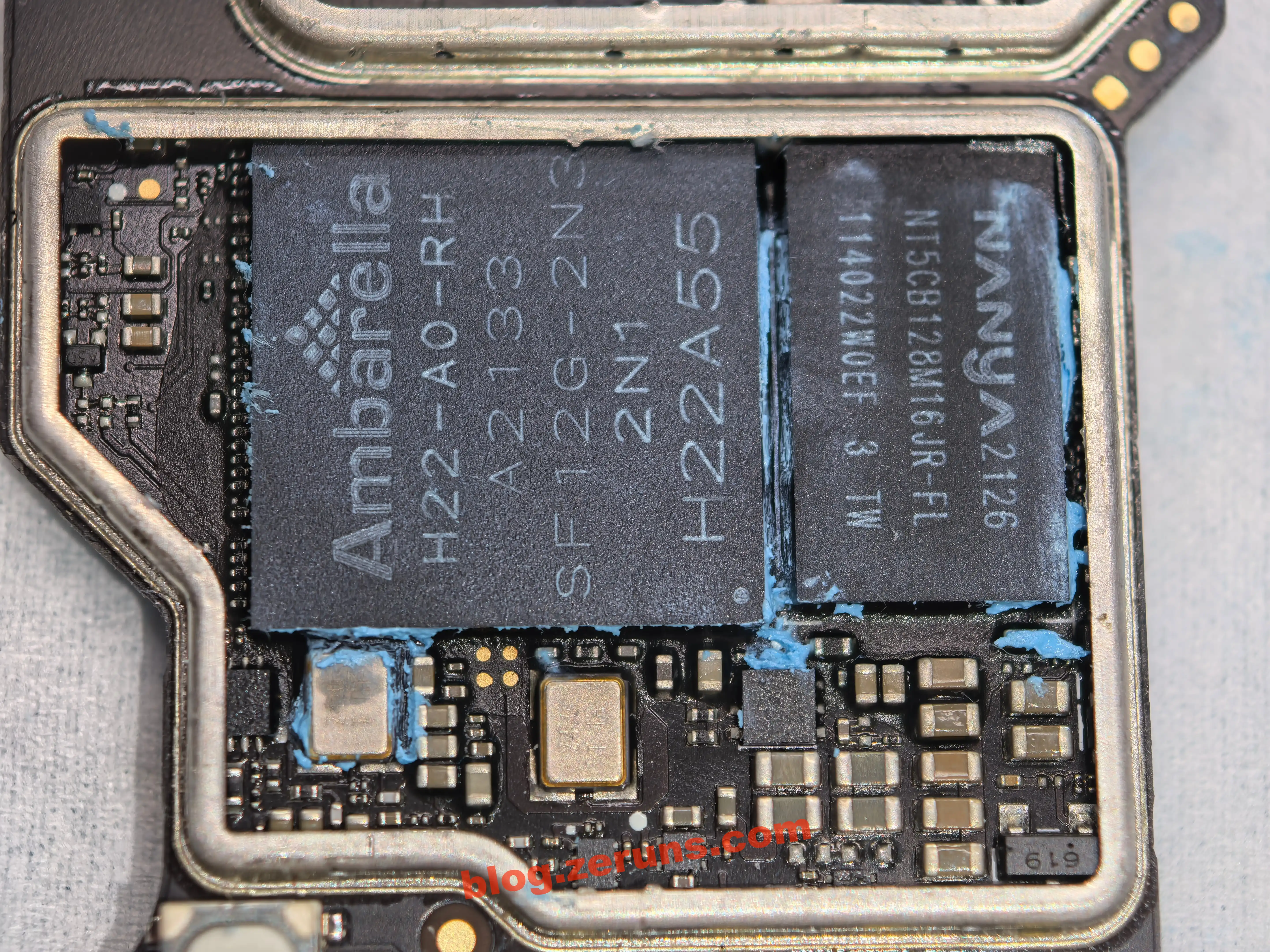
Inside the shield next to the aerial camera interface, there are two main chips: H22-AO-RH and NT5CB128M16JR-FL.
1. Ambarella H22-A0-RH (Video Processing Chip)
Brand and Positioning: Ambarella is a world-leading video processing chip manufacturer, and the H22 series is its high-performance visual processing solution for consumer drones.
Core Architecture and Process:
- CPU: Quad-core ARM Cortex-A53, with a maximum frequency of 1 GHz, supporting multitasking and basic computing.
- Process Technology: 14nm process, balancing performance and power consumption, suitable for long-term operation of portable devices.
- GPU: No independent GPU model is specified, but it integrates a high-performance video DSP that supports 4K video encoding and decoding.
Video Processing Capabilities:
- Encoding Formats: Supports H.265 (HEVC) and H.264 (AVC) encoding, and can output two video streams simultaneously (such as 4K60fps main video + mobile resolution preview stream).
Resolution and Frame Rate:
- Main Video Stream: 4K@60fps (HEVC/AVC).
- Auxiliary Stream: Supports real-time mobile resolution (such as 1080p) WiFi live streaming.
Image Enhancement Technologies:
- 3D Electronic Image Stabilization (EIS): Supports 4K@30fps, achieving stable images through dedicated hardware.
- Multi-exposure HDR: Supports 4K@30fps, improving dynamic range.
- Distortion correction and shutter correction: Optimizing image quality.
2. Nanya NT5CB128M16JR-FL (DDR Memory Chip)
- Brand and Positioning: Nanya Technology is a well-known memory manufacturer, and this model belongs to the DDR3 series.
- Core Parameters:
- Capacity: 128M×16bit (i.e., 2Gbit = 256MByte), operating voltage 1.5V.
- Performance: Provides high-speed data throughput capability to meet the high bandwidth requirements of the Ambarella H22 chip for image caching and algorithm operation.
- Function Role: As running memory, it provides temporary data storage space for the video processing chip, ensuring the smoothness of 4K video encoding and real-time image processing.
These two chips form the visual processing core unit of the drone: the Ambarella H22 is responsible for "processing" high-definition video and executing intelligent algorithms, while the Nanya memory provides a "temporary warehouse" for it. Together, they realize the 4K high-definition image transmission and intelligent visual functions of the DJI drone.
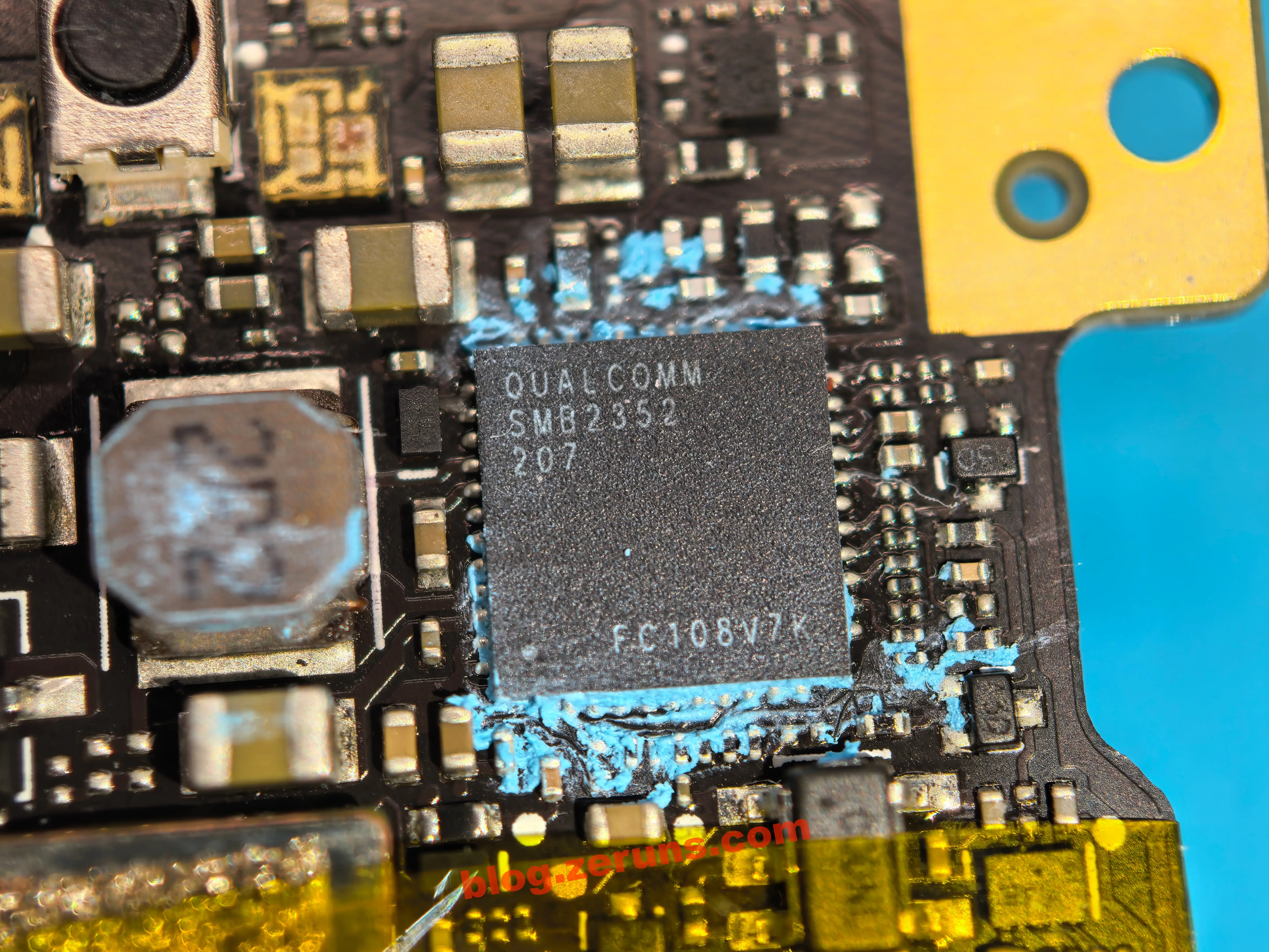
There is a relatively large chip to the right of the Type-C interface, with the model SMB2352.
The SMB2352 is a high-efficiency Buck-Boost charging management IC launched by Qualcomm, mainly used in two-cell battery applications such as power banks, drones, and portable computers. The following are its main technical parameters:
- Input Voltage Range: 3.3V~16.5V (supports USB Type-C input)
- Output Voltage Range: Supports Buck-Boost adjustment, can provide 3.3V~20V power supply for the system
- Maximum Charging Current: Up to 6A at the battery end (programmable adjustment)
- Maximum Input Current: 5A (programmable current limiting)
- Input Power: Up to 45W
- Efficiency: Typical value exceeds 90%
- Packaging: MQFN-57, size 5.5mm × 5.5mm × 0.6mm
- Communication and Control: Supports I²C interface, programmable configuration of charging parameters, protection thresholds, etc.
- Protection Functions: Built-in input overvoltage protection (OVP), input overcurrent protection (OCP), battery over-temperature protection (OTP)
- Protocol Support:
- USB BC 1.2
- Qualcomm Quick Charge 2.0/3.0/4.0
- USB Power Delivery (PD) 3.0 (integrated PD PHY)
- Type-C 1.3 specification
This chip is suitable for high-power density and high-efficiency charging solutions for portable devices, and can flexibly adjust the working mode through an external controller.
Recommended Reading
- Recommended Cost-Effective and Cheap VPS/Cloud Servers: https://blog.zeruns.com/archives/383.html
- Minecraft Server Setup Tutorial: https://blog.zeruns.com/tag/mc/
- 【Open Source】24V3A Flyback Switching Power Supply: https://blog.zeruns.com/archives/910.html
- Simple Unboxing, Review and Teardown of MECHREVO Code10AI Laptop (Ultra7-255H): https://blog.zeruns.com/archives/895.html
- Cross-Border E-Commerce Independent Station Construction Tutorial, WordPress Foreign Trade Website Building Guide: https://blog.zeruns.com/archives/889.html
- Tutorial on Building a PHP Website with Rain Cloud RCA Cloud Application (Based on K8s): https://blog.zeruns.com/archives/869.html


Comment Section