


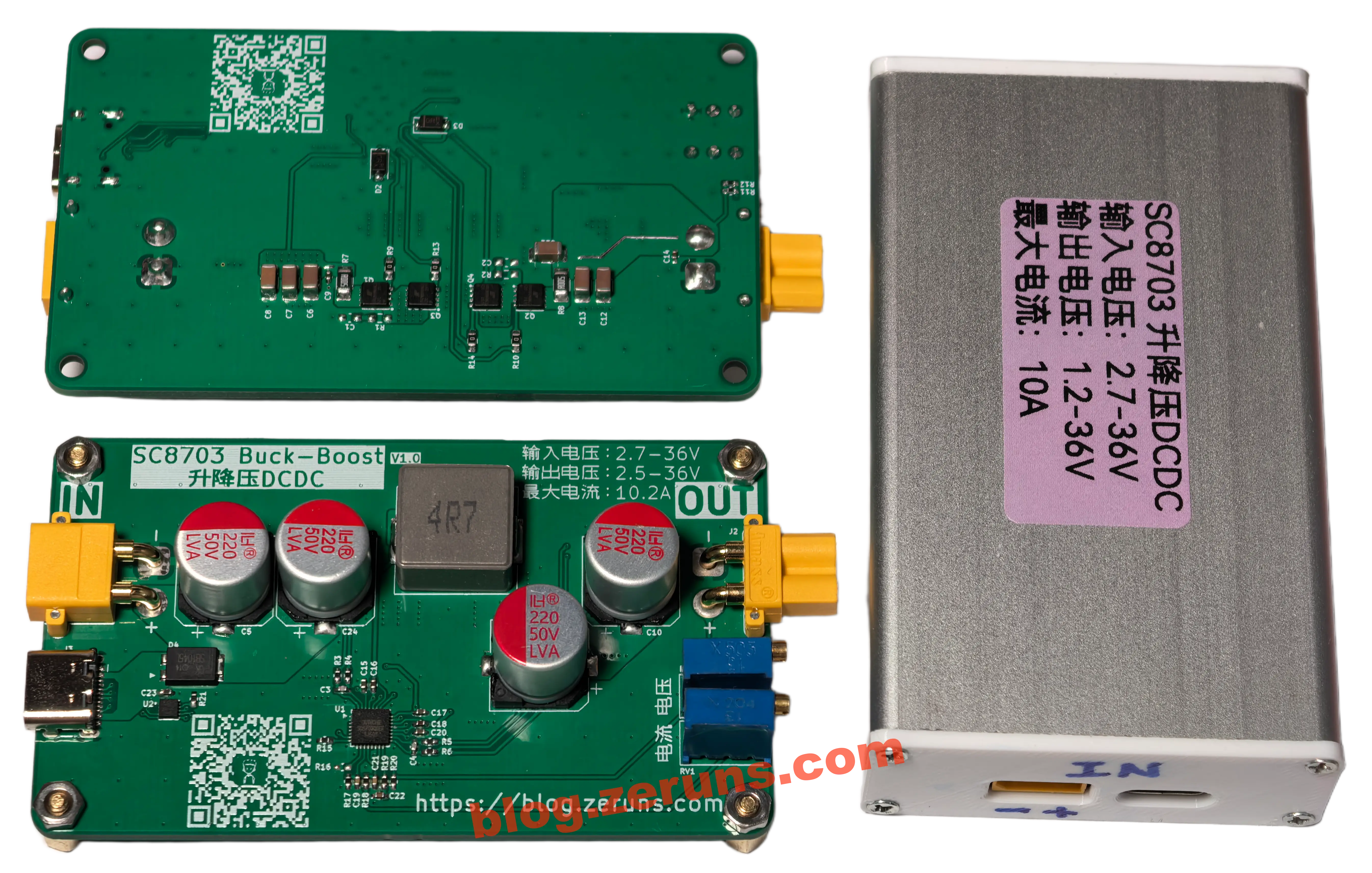
Open sourcing a Buck-Boost DC/DC power module based on the SC8703 chip. Input voltage up to 36V, input/output current up to 10A, switching frequency 600kHz. Output voltage is adjustable, output constant current is adjustable. Maximum conversion efficiency is 95%. Interfaces include XT30 and a Type-C port supporting PD fast charge input (up to 28V PD request).
Design Parameters
| Parameter | Value |
|---|---|
| Input Voltage Range | 2.7V ~ 36V |
| Output Voltage Range | 1.21V ~ 36V |
| Max Input/Output Current | 10A |
| Output CC Adjustable Range | 0.58A ~ 10A |
| Switching Frequency | 600kHz |
| PCB Size | 79.6 x 47 mm |
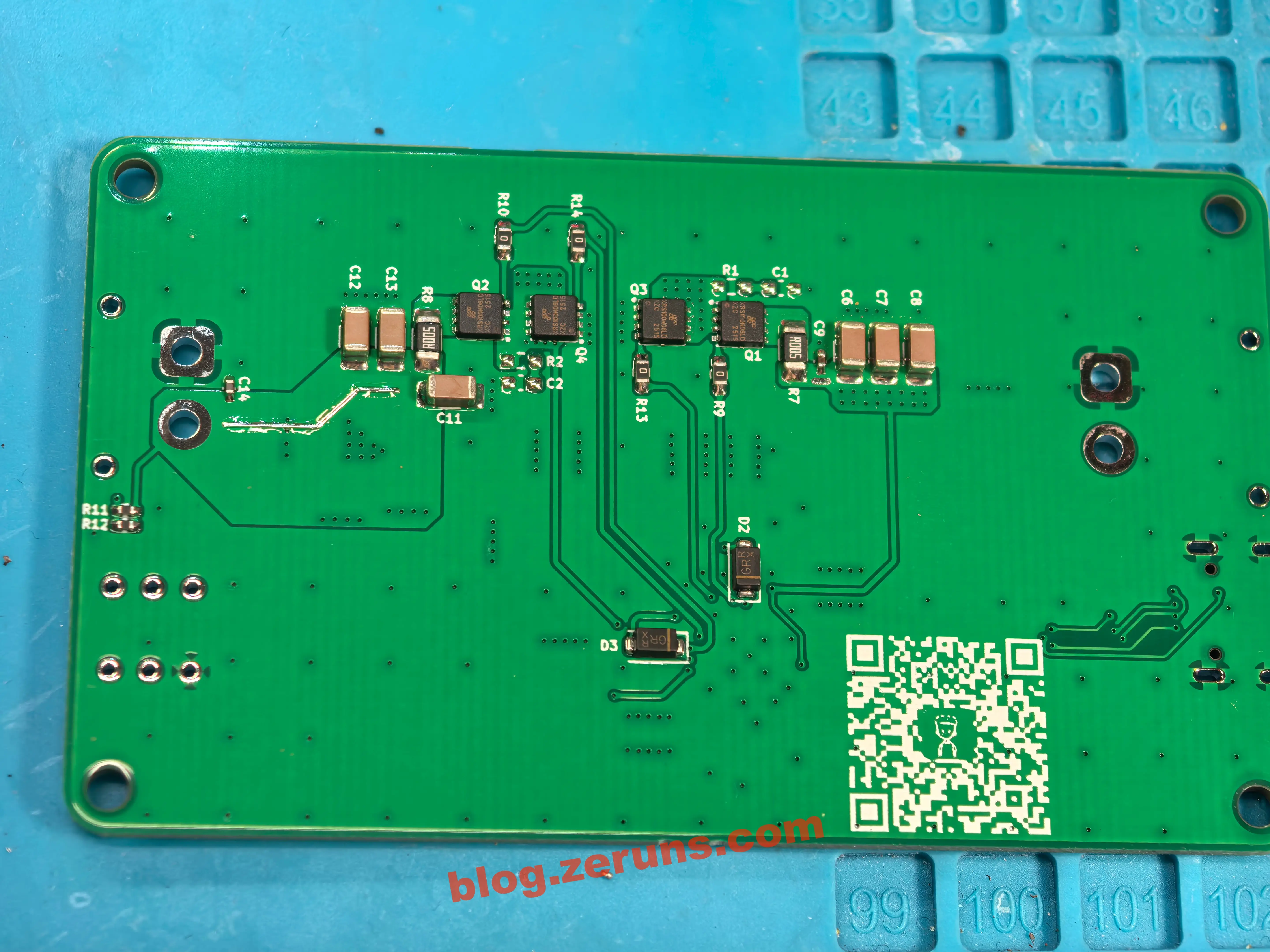
The Buck-Boost power controller chip is SC8703, and the fast charge protocol chip is CH224Q.
Replication Instructions
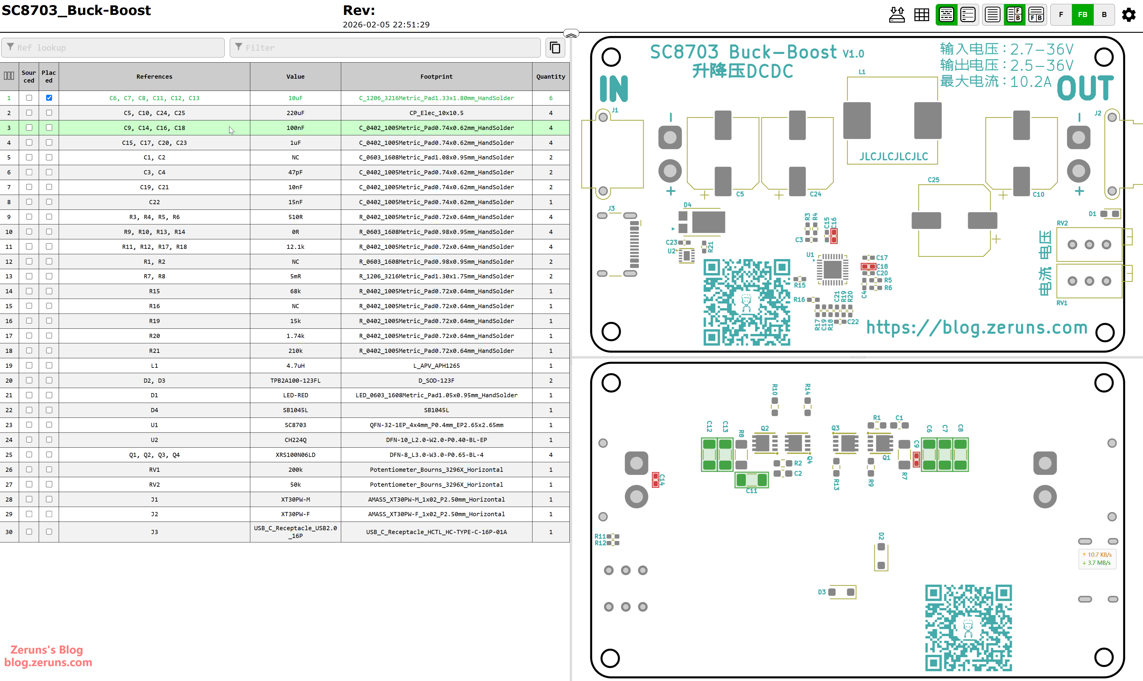
- This project was designed using KiCad. The project on the LCSC (LiChuang) Open Source Platform was imported from KiCad project files, so there might be some issues. It is recommended to use the provided Gerber files directly for PCB orders.
- The project is open-sourced on Gitee, LCSC Open Source Hardware Platform, and Huaqiu Open Source Hardware Community. Links are at the bottom of the article. Provided materials include: KiCad project files, Gerber fabrication files, detailed BOM (with purchase links and prices), combined top/bottom stencil files, SMD silkscreen diagram, Interactive BOM (soldering aid), datasheets for chips used, 3D models of PCBA and enclosure, etc.
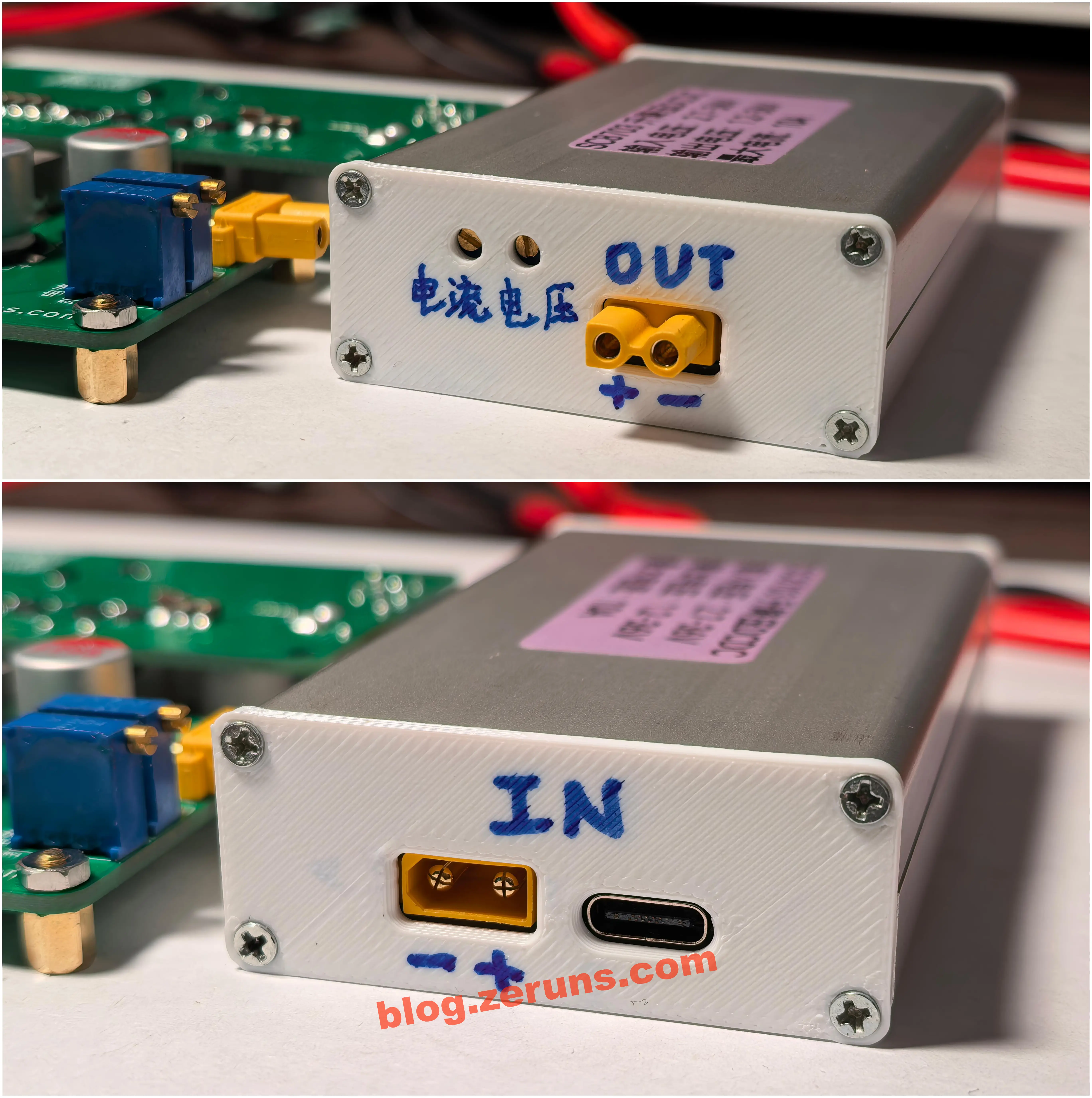
- The enclosure is a commercial aluminum alloy case purchased from Taobao (link in BOM). The front and rear panels are 3D printed; the 3mf model files are included in the materials.
- MOSFETs must contact the enclosure for heat dissipation via thermal silicone pads!
- Recommended operating current for the bare board without heatsink is within 5A!
- The Type-C input and XT30 input interfaces are parallel connection; do not use them simultaneously!
The component cost for small batch production is approximately 30 CNY/set (excluding PCB and enclosure), mainly because the SC8703 chip is expensive, costing around 9 CNY per piece.
▶ Project Video Demo: https://www.bilibili.com/video/BV1mMfPBzEXH/
▶ Electronics/MCU Tech Discussion QQ Group: 2169025065
▶ eeClub - Electronics Engineer Community: https://bbs.eeclub.top/
Please give a Star if you find this useful.
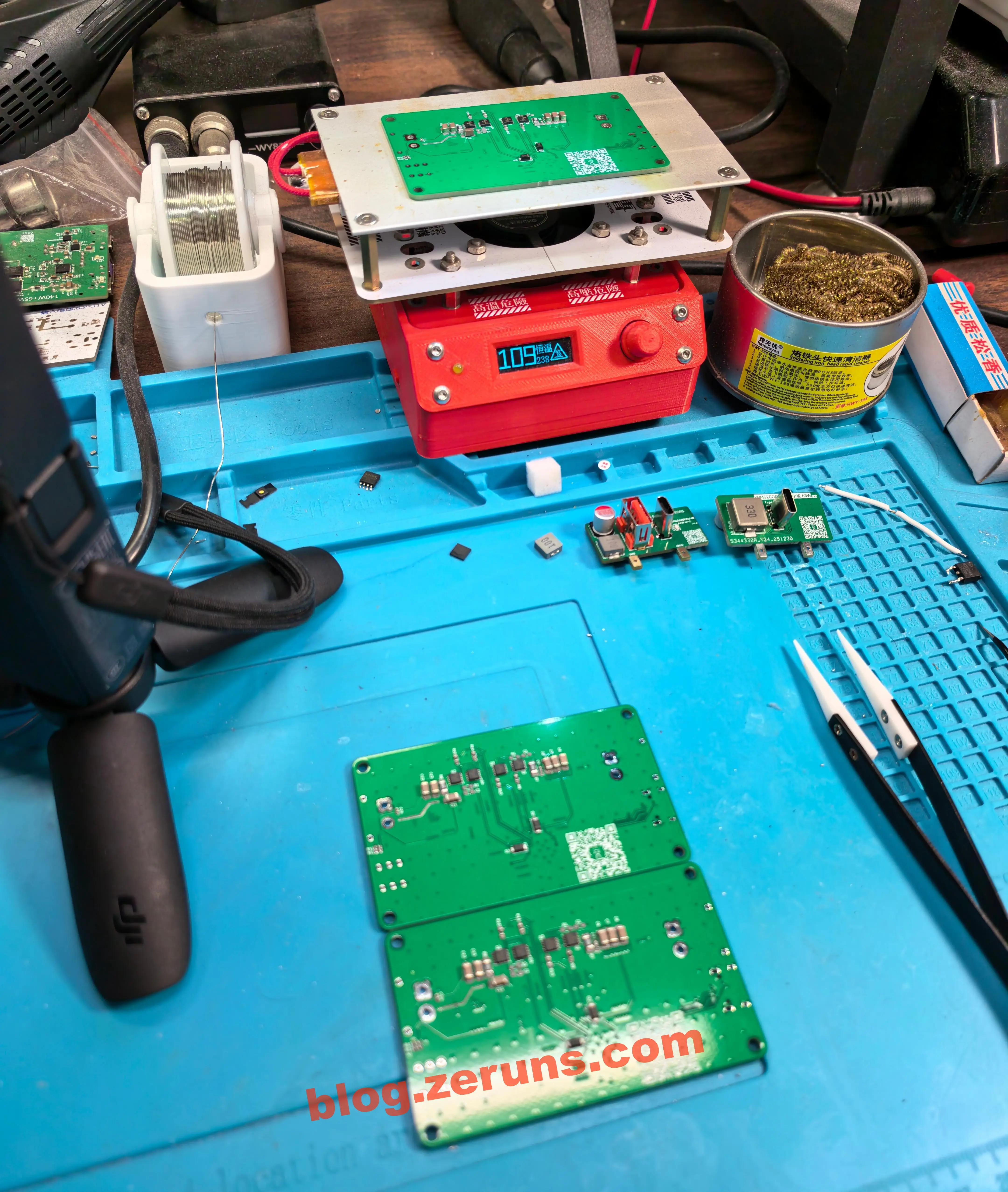
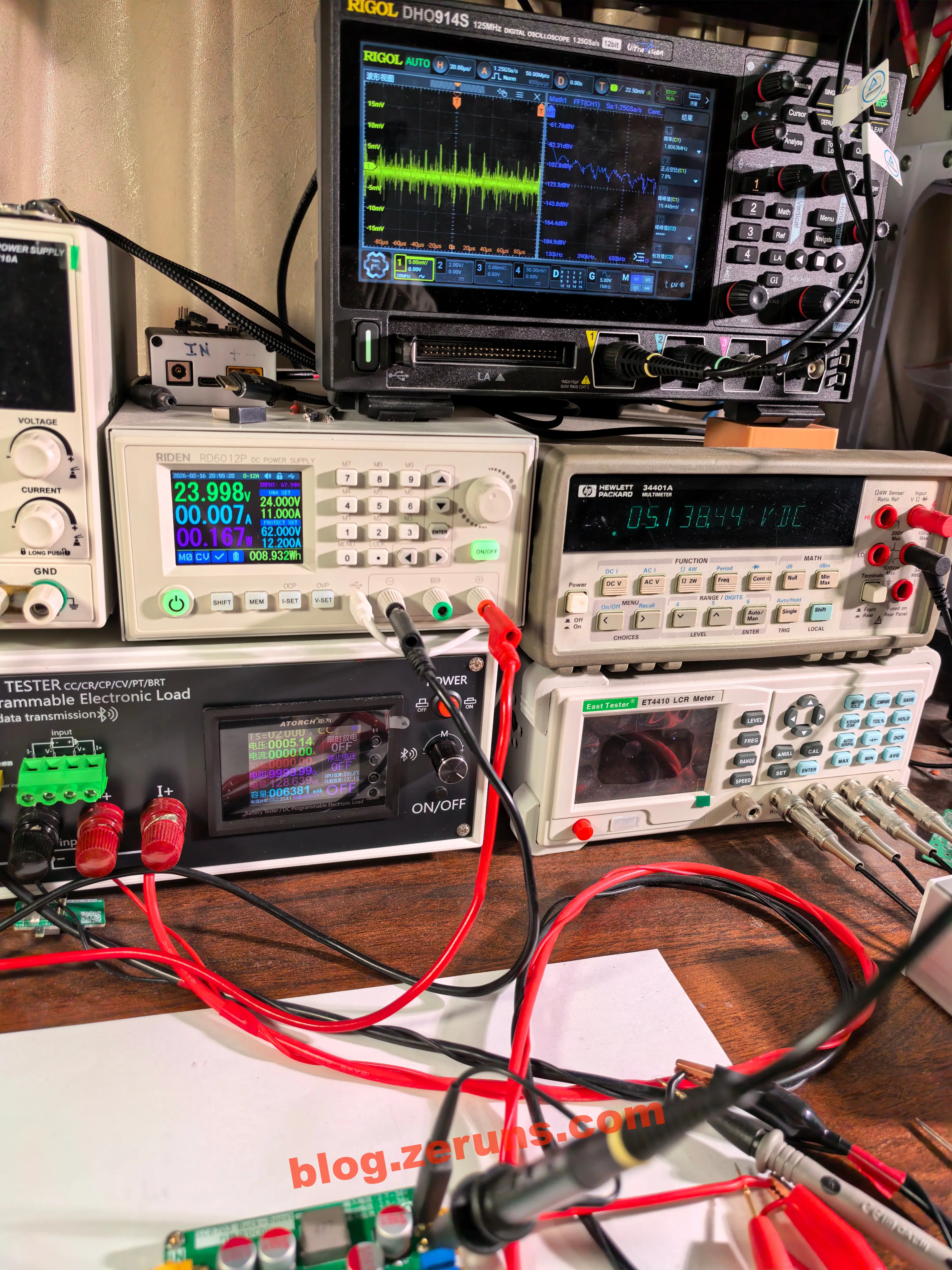
Physical Photos
Soldering Process
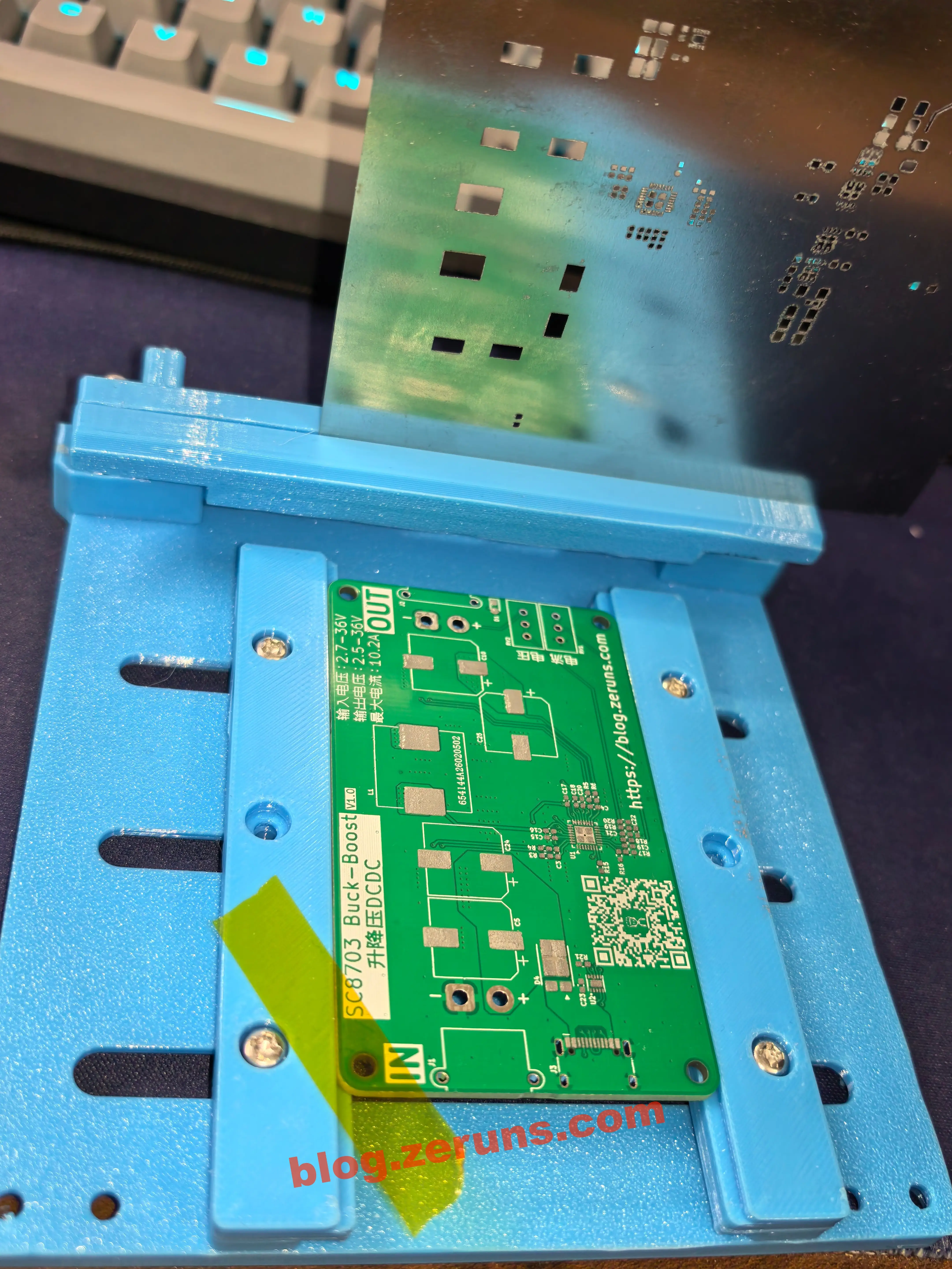
Use the provided stencil files to order a 10x10 stencil from Taobao (approx. 15 CNY). 3D print a jig for applying solder paste. Align the stencil with the PCB, apply the paste, place components according to the Interactive BOM, and then use a hotplate or reflow oven. It is recommended to solder the bottom layer first, then the top layer.

Testing
Power-on test: Input 12V, Output 24V. No-load power consumption is approx 0.37W.
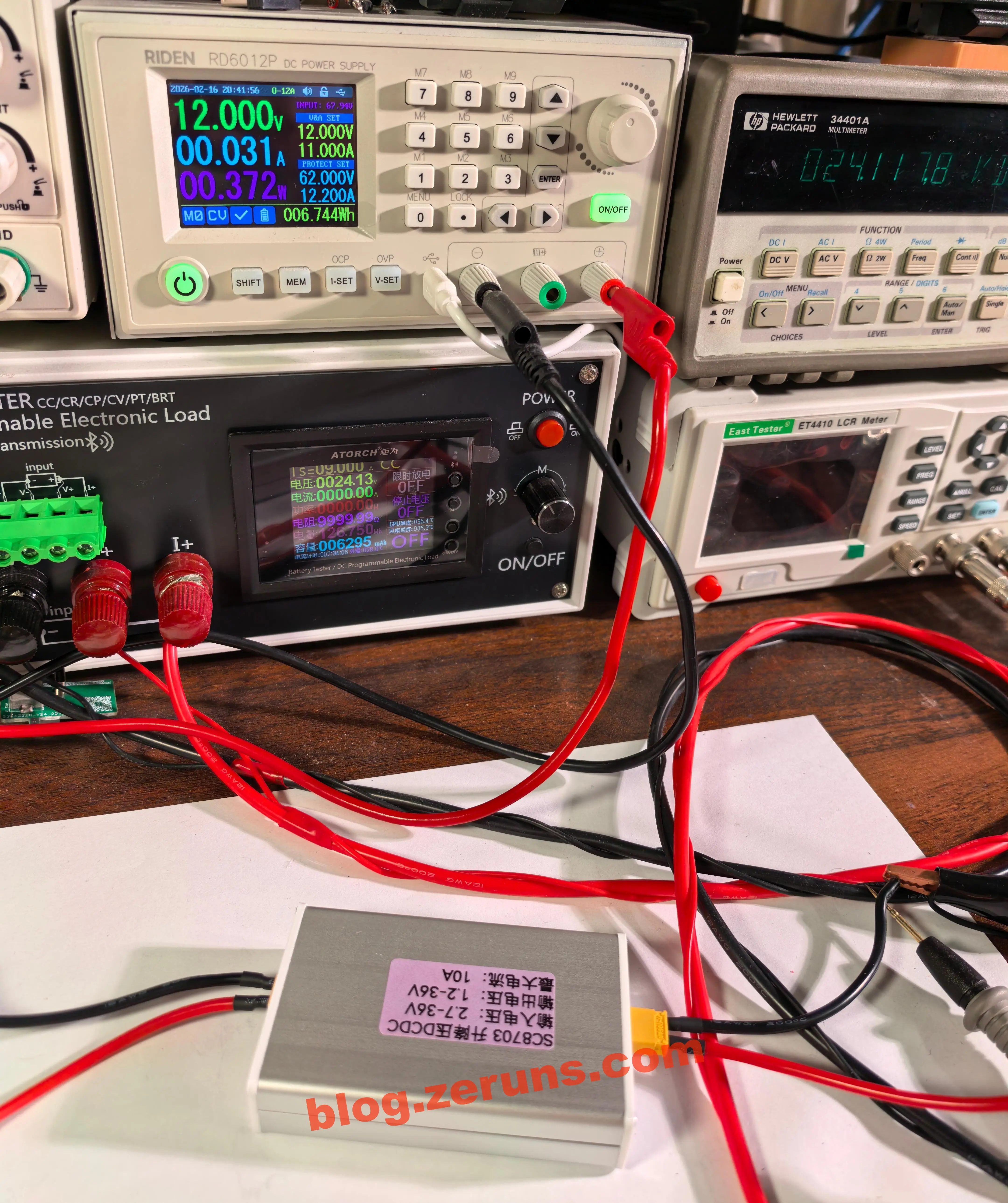
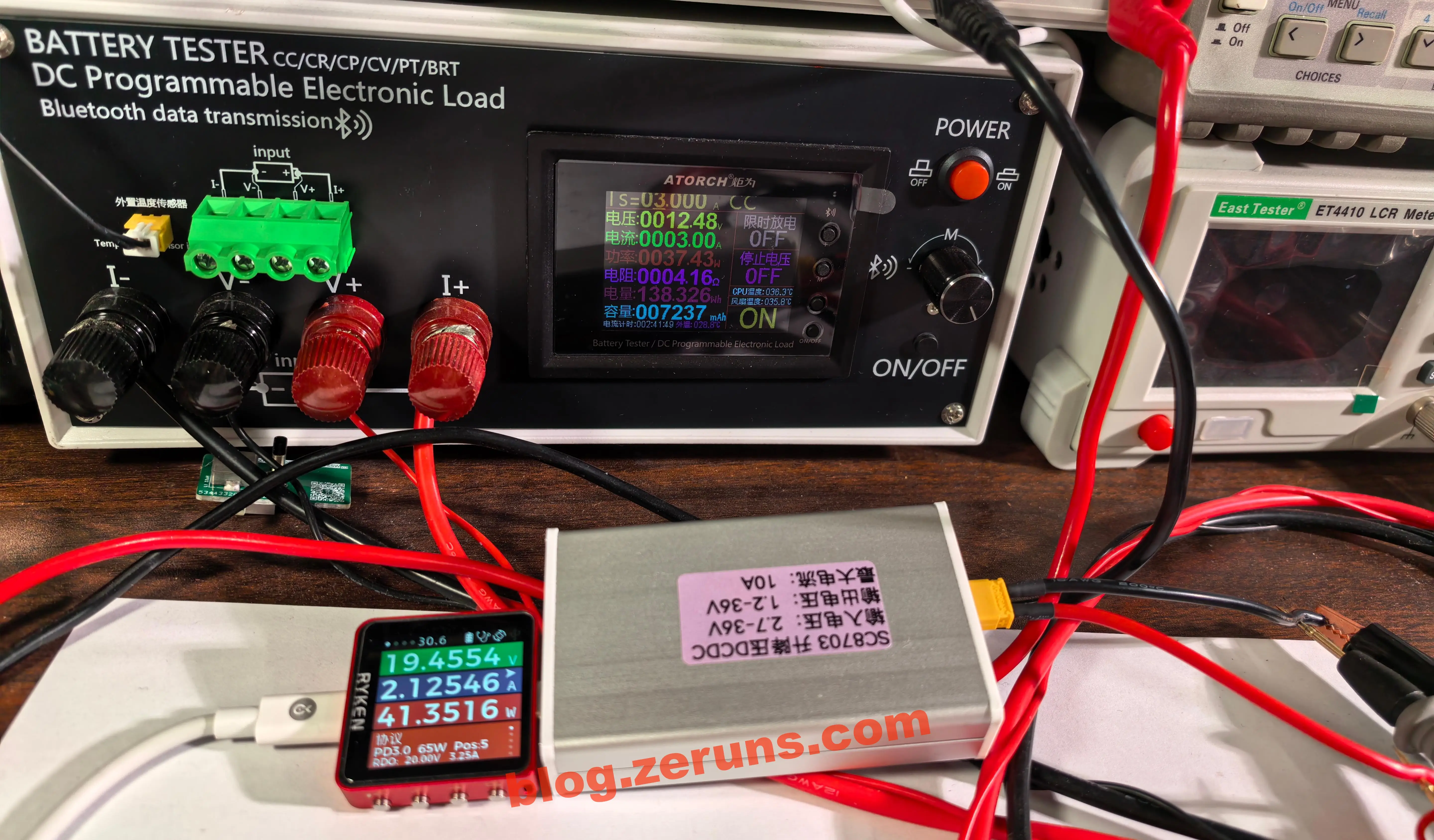
Type-C input test: Using a 65W PD charger, successfully requested (spoofed) 20V.
Conversion Efficiency Test
Ruiden RD6012P Programmable Power Supply Simple Review: https://blog.zeruns.com/archives/740.html

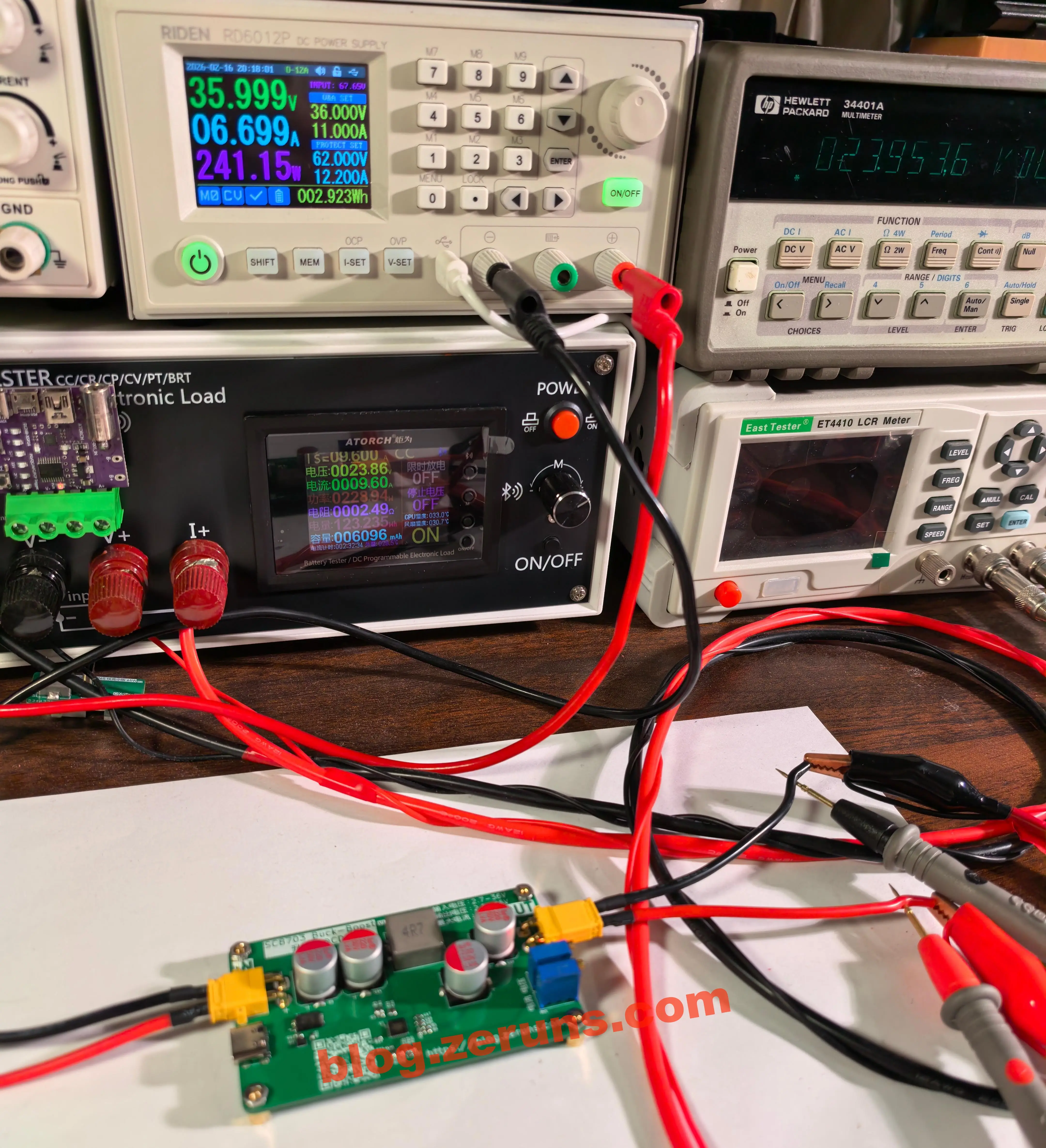
Measured maximum conversion efficiency: 95.45%
| Input Voltage(V) | Input Current(A) | Input Power(W) | Output Voltage(V) | Output Current(A) | Output Power(W) | Efficiency(%) |
|---|---|---|---|---|---|---|
| 35.999 | 0.752 | 27.071 | 24.130 | 1.000 | 24.130 | 89.14% |
| 35.999 | 6.699 | 241.157 | 23.954 | 9.600 | 229.955 | 95.35% |
| 5.000 | 9.063 | 45.315 | 24.028 | 1.500 | 36.042 | 79.54% |
| 5.000 | 8.520 | 42.600 | 12.054 | 3.000 | 36.162 | 84.89% |
| 12.000 | 4.382 | 52.584 | 5.230 | 9.000 | 47.070 | 89.51% |
| 11.999 | 8.753 | 105.027 | 24.048 | 4.000 | 96.192 | 91.59% |
| 5.000 | 9.803 | 49.015 | 19.990 | 2.000 | 39.980 | 81.57% |
| 5.000 | 5.063 | 25.315 | 21.116 | 1.000 | 21.116 | 83.41% |
| 11.999 | 6.705 | 80.453 | 35.477 | 2.000 | 70.954 | 88.19% |
| 35.999 | 3.459 | 124.521 | 11.998 | 9.510 | 114.097 | 91.63% |
| 35.999 | 1.839 | 66.202 | 12.023 | 5.000 | 60.116 | 90.81% |
| 35.999 | 9.288 | 334.359 | 35.460 | 9.000 | 319.141 | 95.45% |
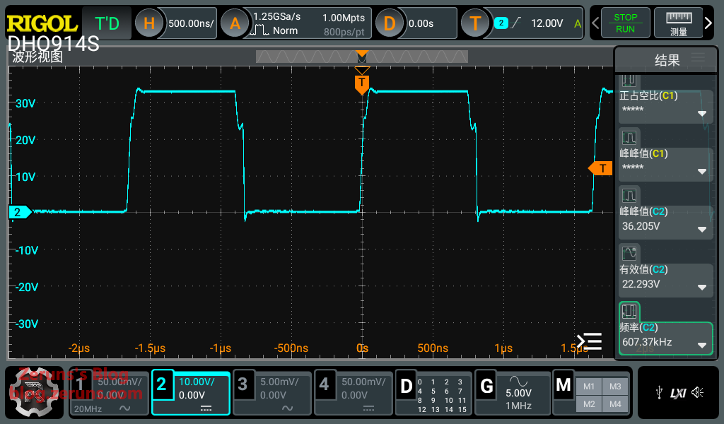
MOS Gate Drive Waveforms
Input Side (Buck Section) MOS High-Side Gate to Ground Waveform:
Switching frequency 607kHz, period approx 1.65 microseconds. Miller plateau duration approx 20ns. Normal behavior. The drive waveform is clean with no ringing and very small overshoot.
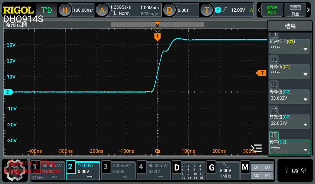
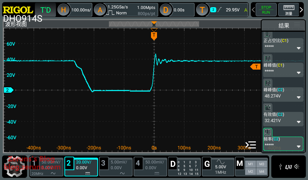
Output Side (Boost Section) MOS High-Side Gate to Ground Waveform:
Switching frequency 607kHz, period approx 1.65 microseconds. Overshoot and ringing exist during MOS turn-on, likely due to driver trace layout issues.
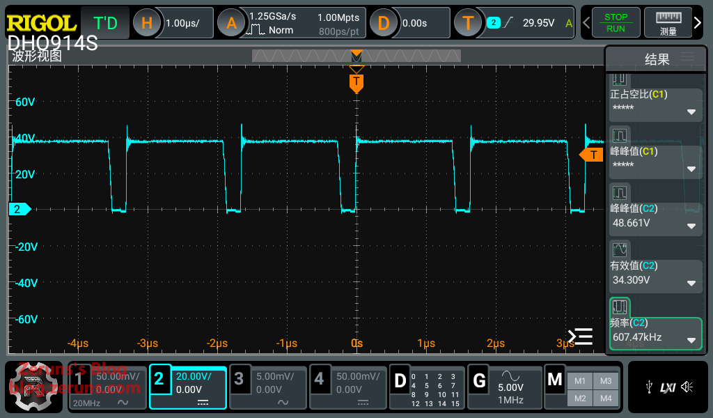
Ripple Test
RIGOL DHO914S Oscilloscope Simple Review: https://blog.zeruns.com/archives/764.html
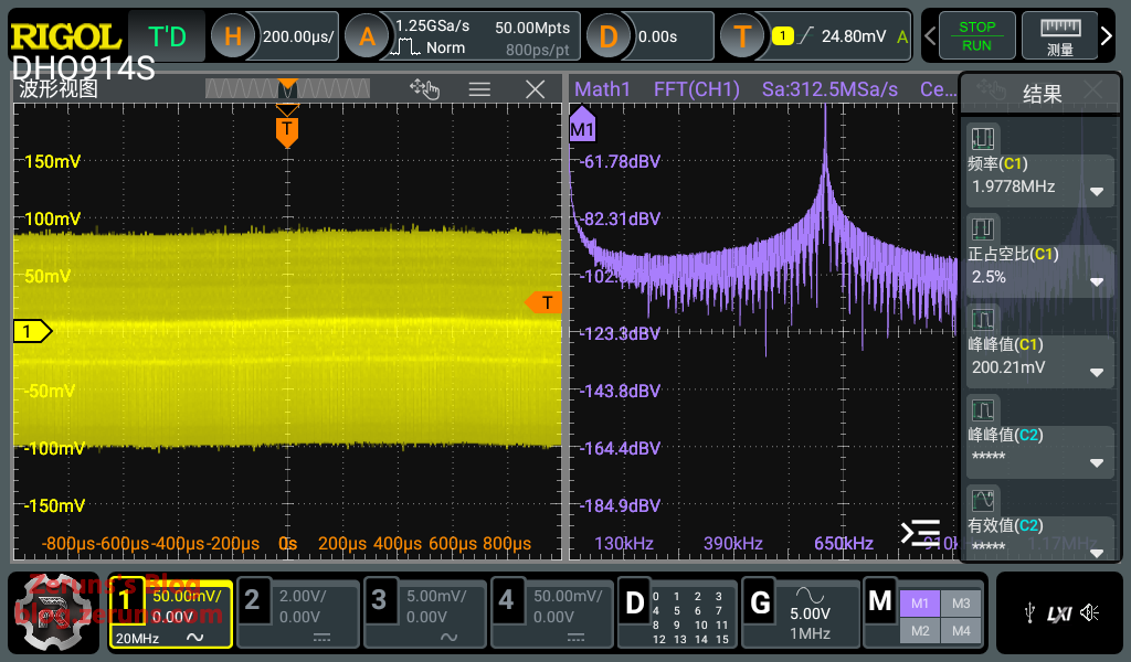
Input 12V, Output 24V No-load: Measured ripple peak-to-peak value approx 60mV.
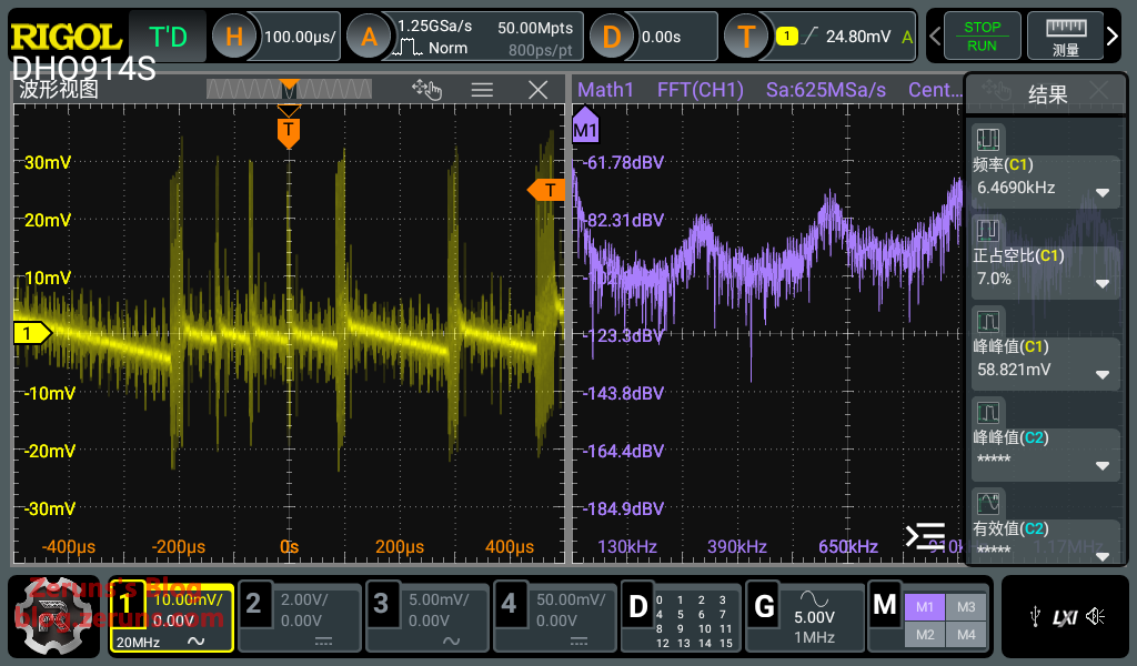
Input 12V, Output 24V/2A Load: Measured ripple peak-to-peak value approx 200mV.
Input 24V, Output 5V No-load: Measured ripple peak-to-peak value approx 16mV.
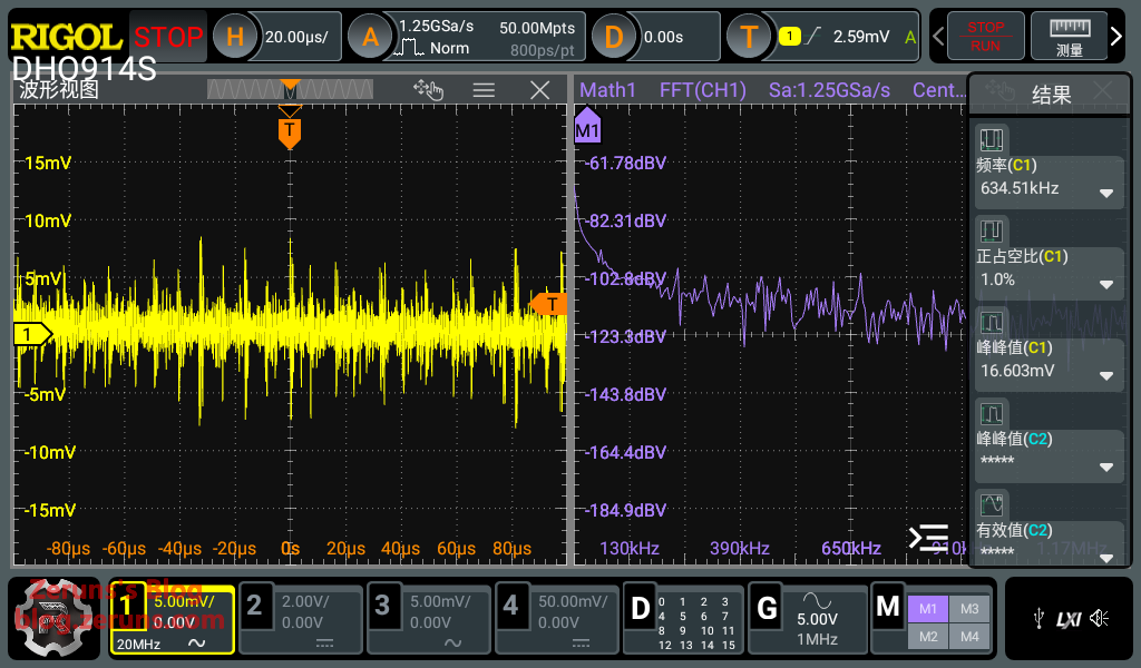
Input 24V, Output 5V/2A Load: Measured ripple peak-to-peak value approx 35mV.


Thermal Imaging
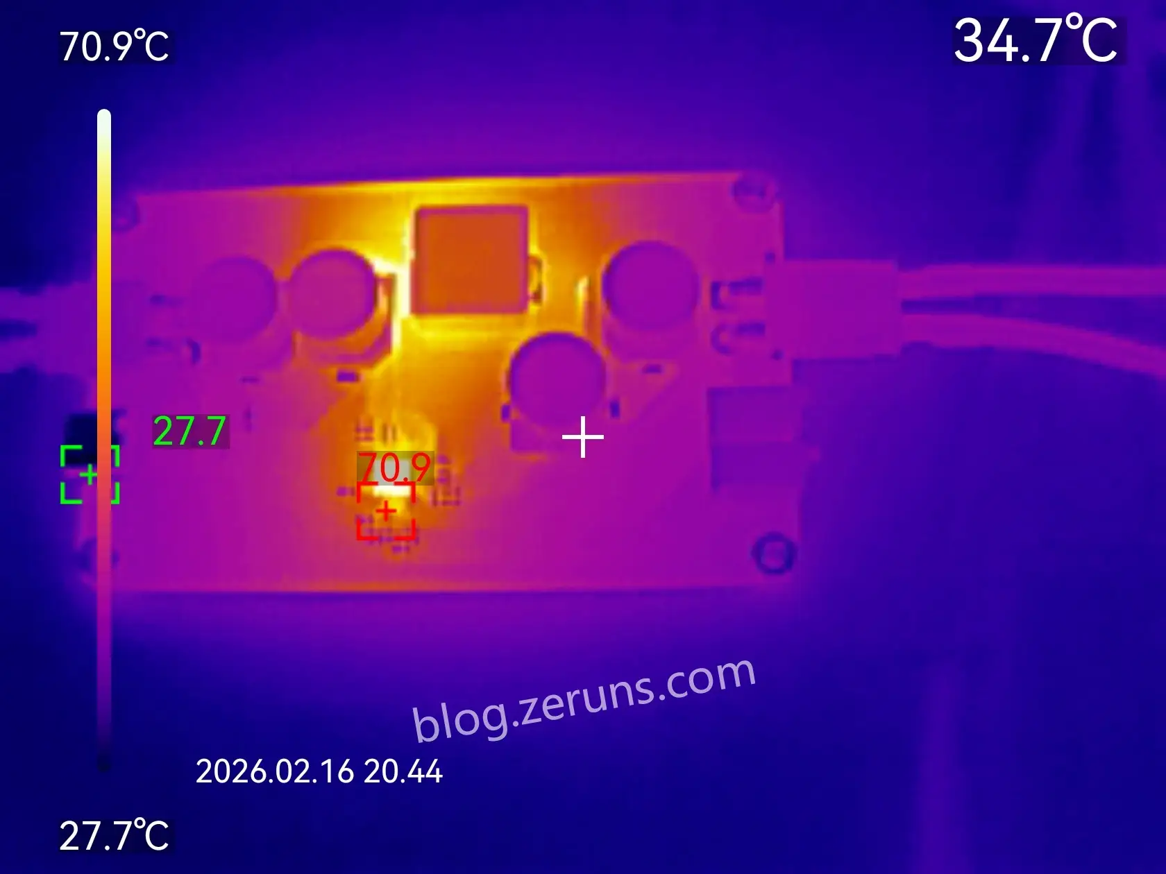
Without any heatsink: Input 36V, Output 24V/9.5A. MOS temperature rose above 100°C within 5 seconds. Bottom side thermal image below.
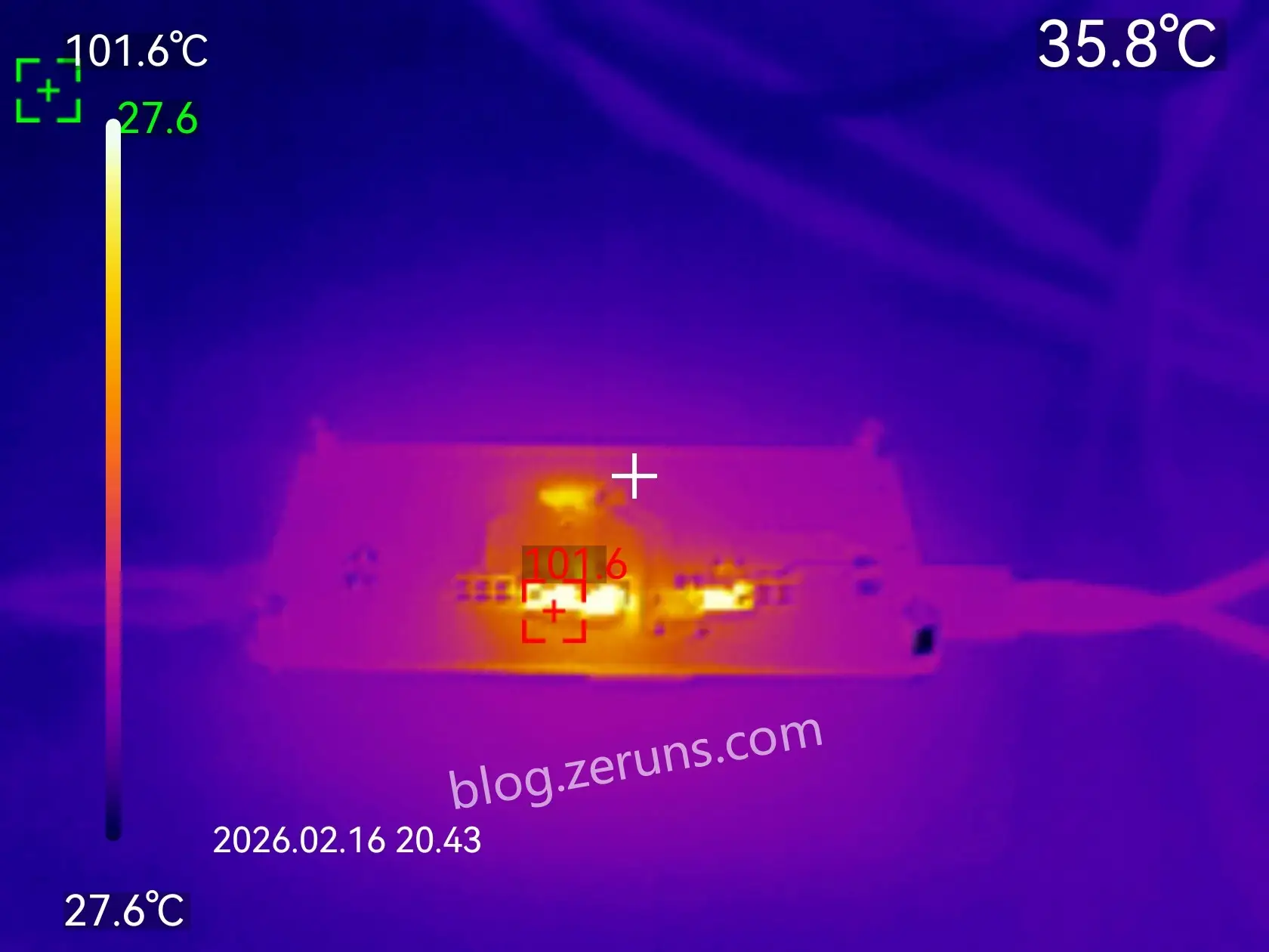
Front side thermal image: SC8703 chip temperature above 70°C.
Thermal image after installing aluminum alloy enclosure:
Since the aluminum alloy is somewhat reflective, which affects measurement results, a piece of tape was applied to the center. The maximum temperature on the side contacting the MOSFETs was measured at approx 53°C.

Download Links
Provided materials include: KiCad project files, Gerber fabrication files, detailed BOM (with purchase links and prices), combined top/bottom stencil files, SMD silkscreen diagram, Interactive BOM (soldering aid), datasheets for chips used, 3D models of PCBA and enclosure, etc.
- Gitee Open Source Address: https://gitee.com/zeruns/sc8703_-buck-boost
- Github Open Source Address: https://github.com/zeruns/sc8703_-buck-boost
- LCSC Open Source Platform Address: https://oshwhub.com/zeruns/sc8703_buck-boost
- Huaqiu Open Source Platform Address: https://p.eda.cn/d-1341729185952956416
- 123 Cloud Drive Download: https://www.123865.com/s/2Y9Djv-I9ddH
Recommended Open Source Projects
- Made a three-phase electricity meter and open-sourced it for easy home energy monitoring: https://blog.zeruns.com/archives/771.html
- STM32-based Synchronous Rectification Buck-Boost Digital Power Supply (Open Source): https://blog.zeruns.com/archives/791.html
- LM25118 Automatic Buck-Boost Adjustable DC/DC Power Module: https://blog.zeruns.com/archives/727.html
- CH32V307-based Smart Electronic Load (Open Source), Embedded Competition Entry: https://blog.zeruns.com/archives/785.html
- EG1151 High Power Synchronous Rectification Adjustable Buck-Boost Power Module (Type-C PD Input Support) Open Source: https://blog.zeruns.com/archives/794.html
- Open Source 140W+65W Buck-Boost PD3.1 Fast Charge Module (2C+1A), IP6557+IP6538, 205W Desktop Charger: https://blog.zeruns.com/archives/801.html
- Open Source Type-C Docking Station, 4x 10Gbps USBA + 2.5G Ethernet + Card Reader: https://blog.zeruns.com/archives/868.html
- [Open Source] 24V3A Flyback Switching Power Supply (Based on UC3842, includes circuit and transformer calculation): https://blog.zeruns.com/archives/910.html
Recommended Reading
- High Cost-Performance and Cheap VPS/Cloud Server Recommendations: https://blog.zeruns.com/archives/383.html
- Minecraft Server Setup Tutorial: https://blog.zeruns.com/tag/mc/
- GL-RM1PE Simple Unboxing Review and Teardown, Enabling BMC Remote Management for Ordinary PCs: https://blog.zeruns.com/archives/900.html
- Discourse Forum Setup Tutorial, Zero-Basis Deployment of Discourse Open Source Community Forum Website: https://blog.zeruns.com/archives/919.html
- OWON HDS160 Oscilloscope Multimeter Simple Unboxing Review and Teardown: https://blog.zeruns.com/archives/927.html
- Minecraft One-Click Quick Server Setup Tutorial, Supports Various MC Versions (forge, fabric, paper, bedrock, etc.): https://blog.zeruns.com/archives/923.html


Comment Section