We are open-sourcing a fully domestic high-power adjustable buck-boost DC-DC power module based on the EG1151 chip. It supports Type-C input, includes PD3.1 triggering with up to 48V, XT60 and DC5.5 input interfaces, a maximum input/output voltage of 63V, and up to 20A input/output current. It also features overcurrent and over-temperature protection, achieving a maximum efficiency of 96.8%.
All components used in this module are domestically produced.
The PD3.1 triggering chip used is the FS312BH, which can request up to 48V from a PD charger. If the charger doesn’t support this voltage, the chip will automatically select the closest available voltage. For instance, if your PD charger supports a maximum of 28V, it will output 28V. (At the time of writing, most PD3.1 chargers on the market seem to max out at 28V.)
To achieve 28V input through the Type-C interface, your charger must support PD3.1 28V, and your cable must include an E-mark chip supporting the PD3.1 ERP28V protocol.
Note: Do not use multiple input interfaces simultaneously as the input ports are connected in parallel!
Demo video: https://www.bilibili.com/video/BV1fS411P7Cp/
Download links for resources are provided at the end of the article!
Although the module is designed for a maximum current of 20A, testing shows that it can only sustain up to around 18A. At 18A, the voltage drop becomes quite noticeable!
This is just a modest attempt. Constructive feedback and suggestions for improvement are welcome in the comments section for friendly discussions.
Open source link on LCSC platform: https://oshwhub.com/zeruns/eg1151-da-gong-lv-tong-bu-zheng-liu-sheng-jiang-ya-mo-kuai-zhi-chi-typec-pd-kuai-chong-shu-ru
Electronics/Microcontroller Technology Exchange QQ Group: 820537762
Introduction to EG1151
The EG1151 is a four-switch buck-boost DC-DC power management chip that integrates functions like reference voltage, oscillator, error amplifier, current limit protection, short-circuit protection, half-bridge driver, and more. It adjusts control strategies based on the specific relationship between input and output voltage and different load conditions. This chip ensures stable voltage output across a wide input voltage range and is ideal for scenarios requiring buck-boost conversions with high currents, especially where battery power provides non-constant voltage. It also supports battery charging.
Features:
- Wide input voltage range: 7V–150V
- High efficiency, up to 95%
- Undervoltage protection
- Over-temperature protection
- Battery charging support
- Output short-circuit protection
- Package: QFN32
Images of the Module
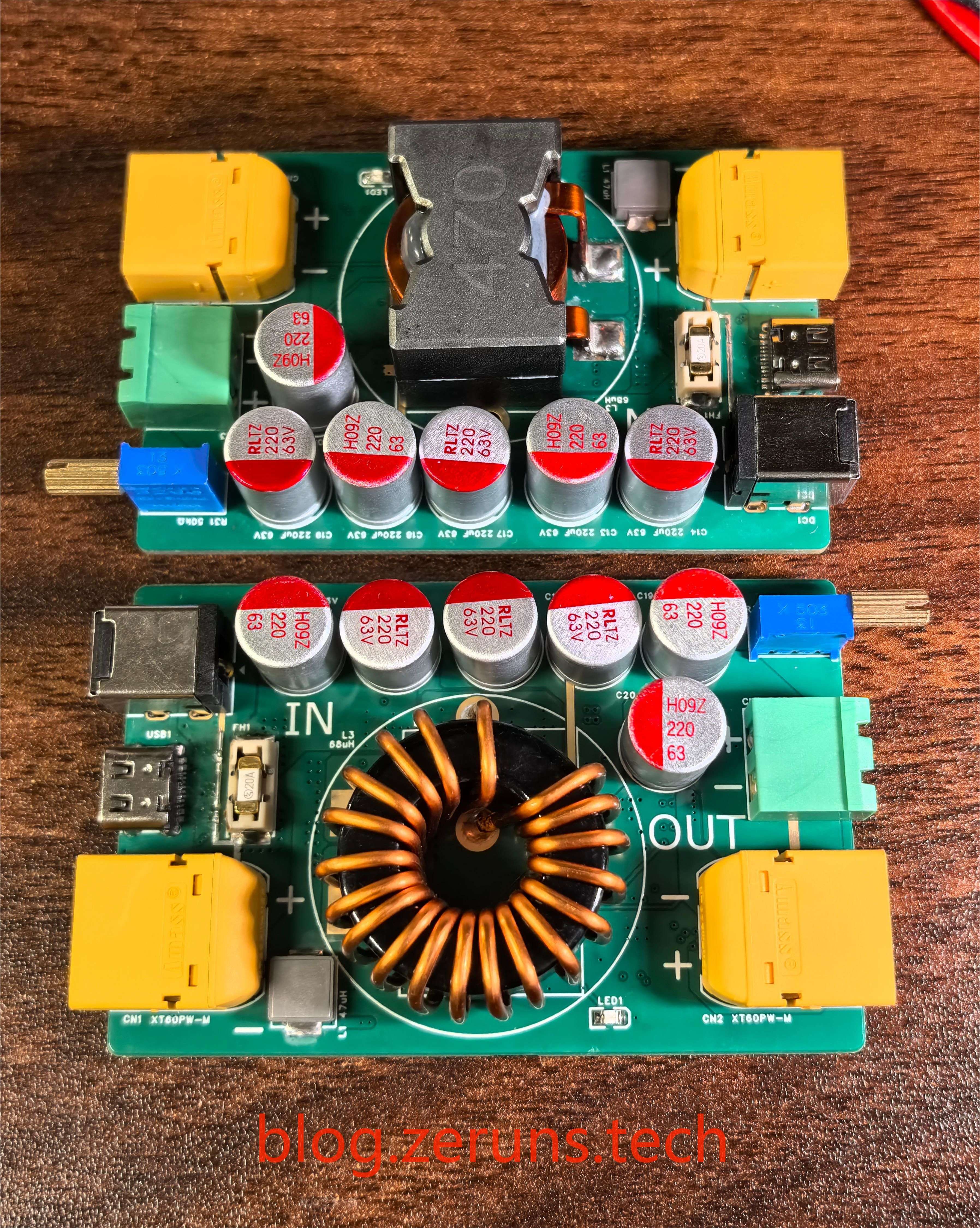
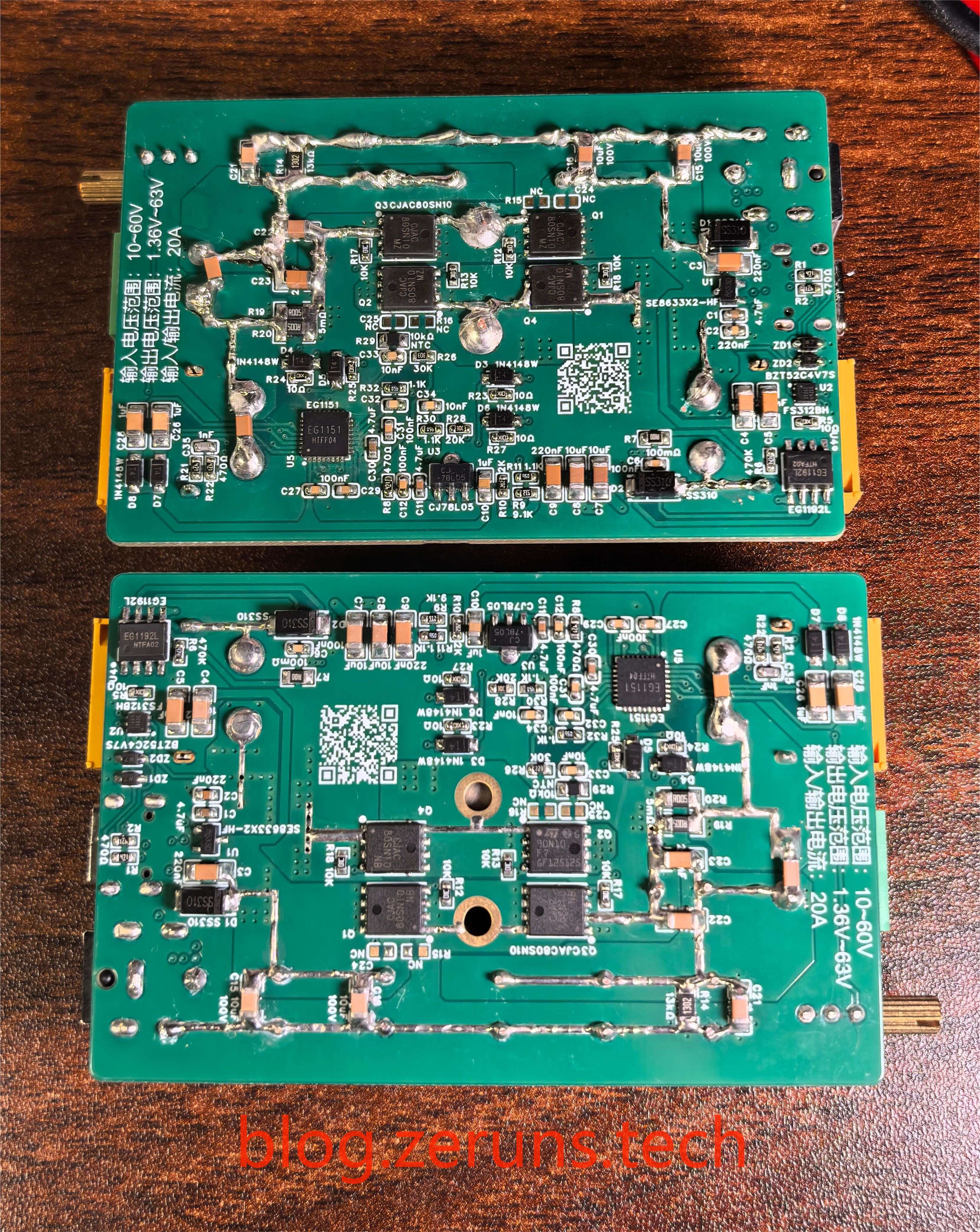
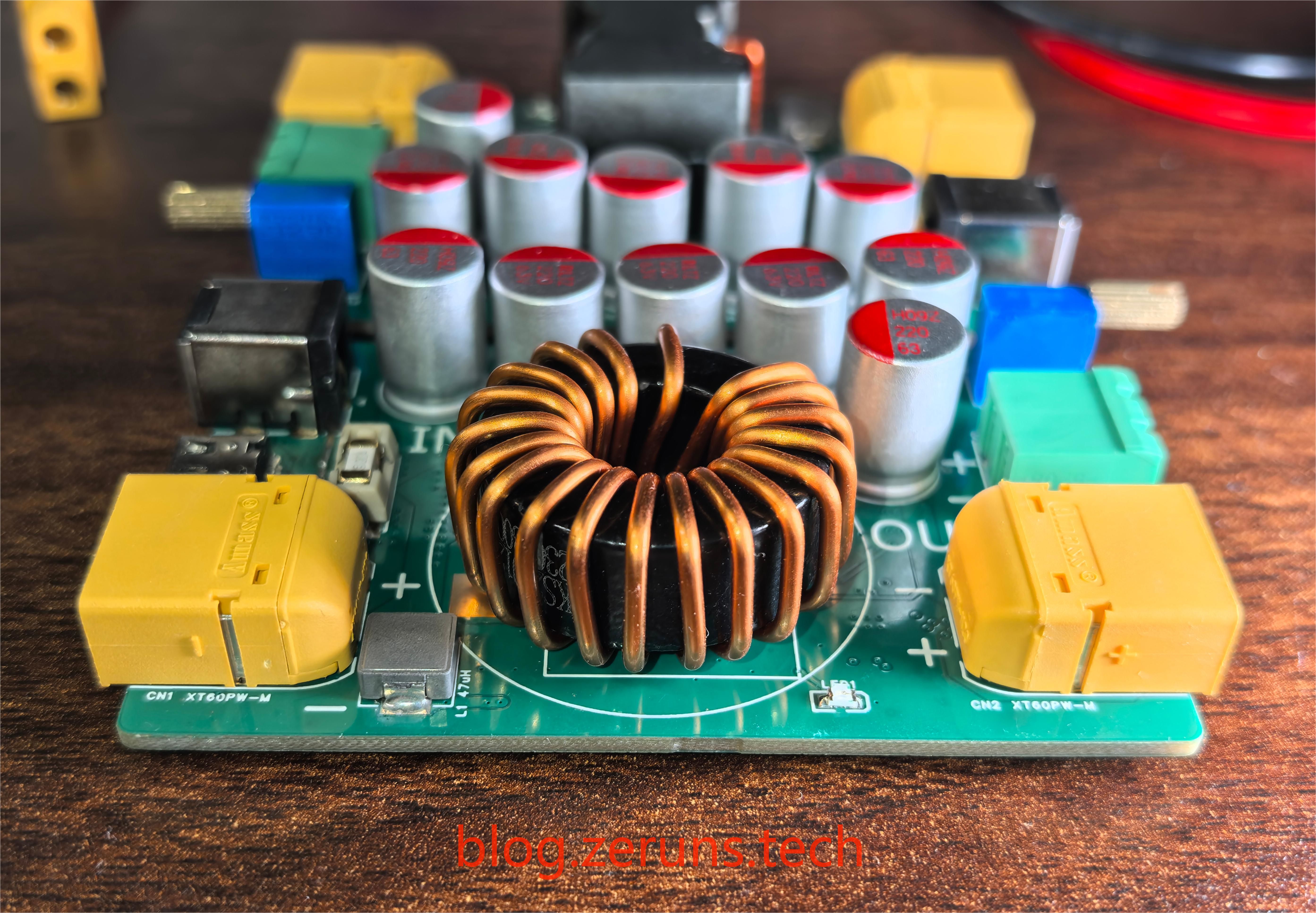
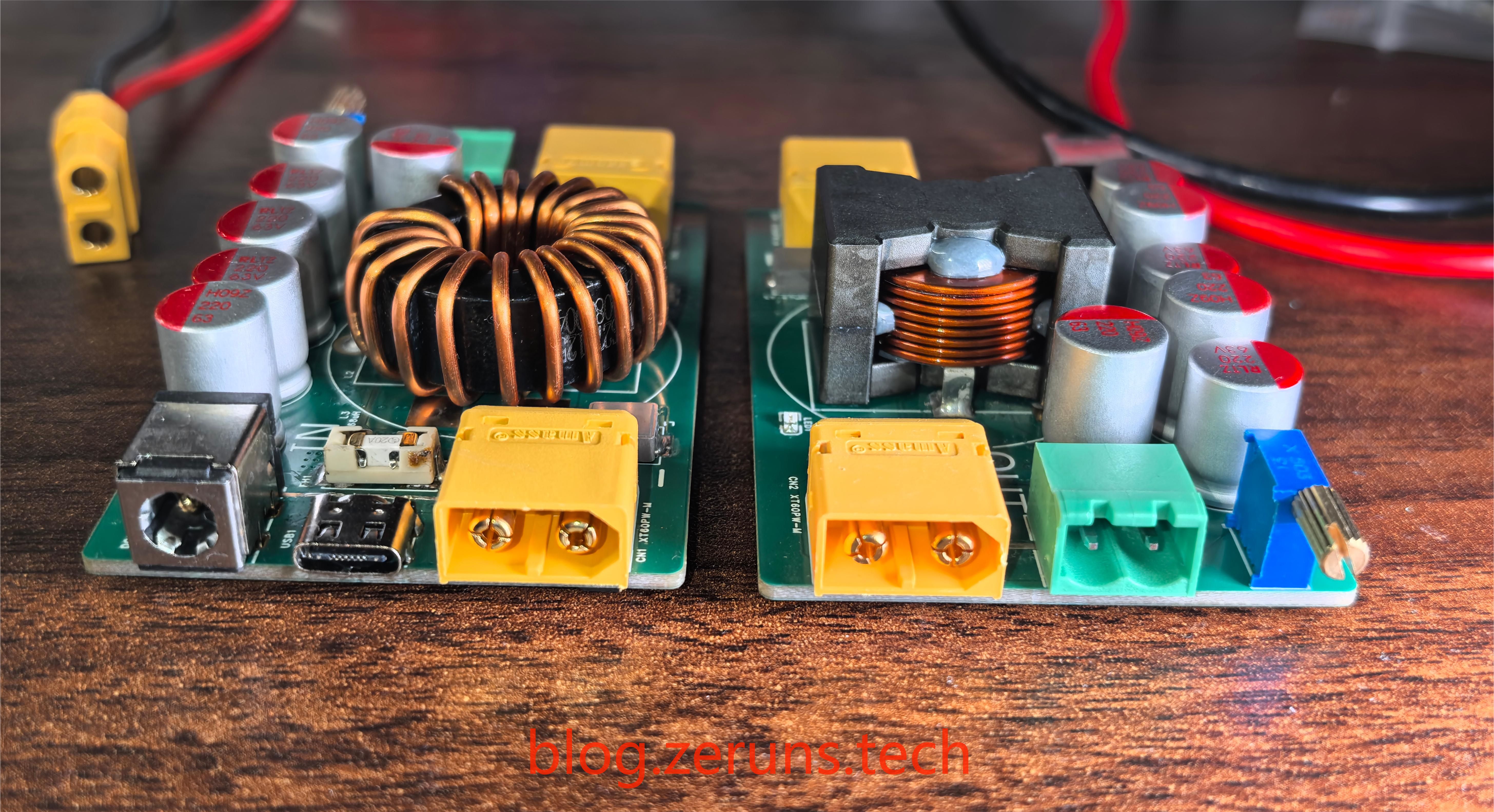
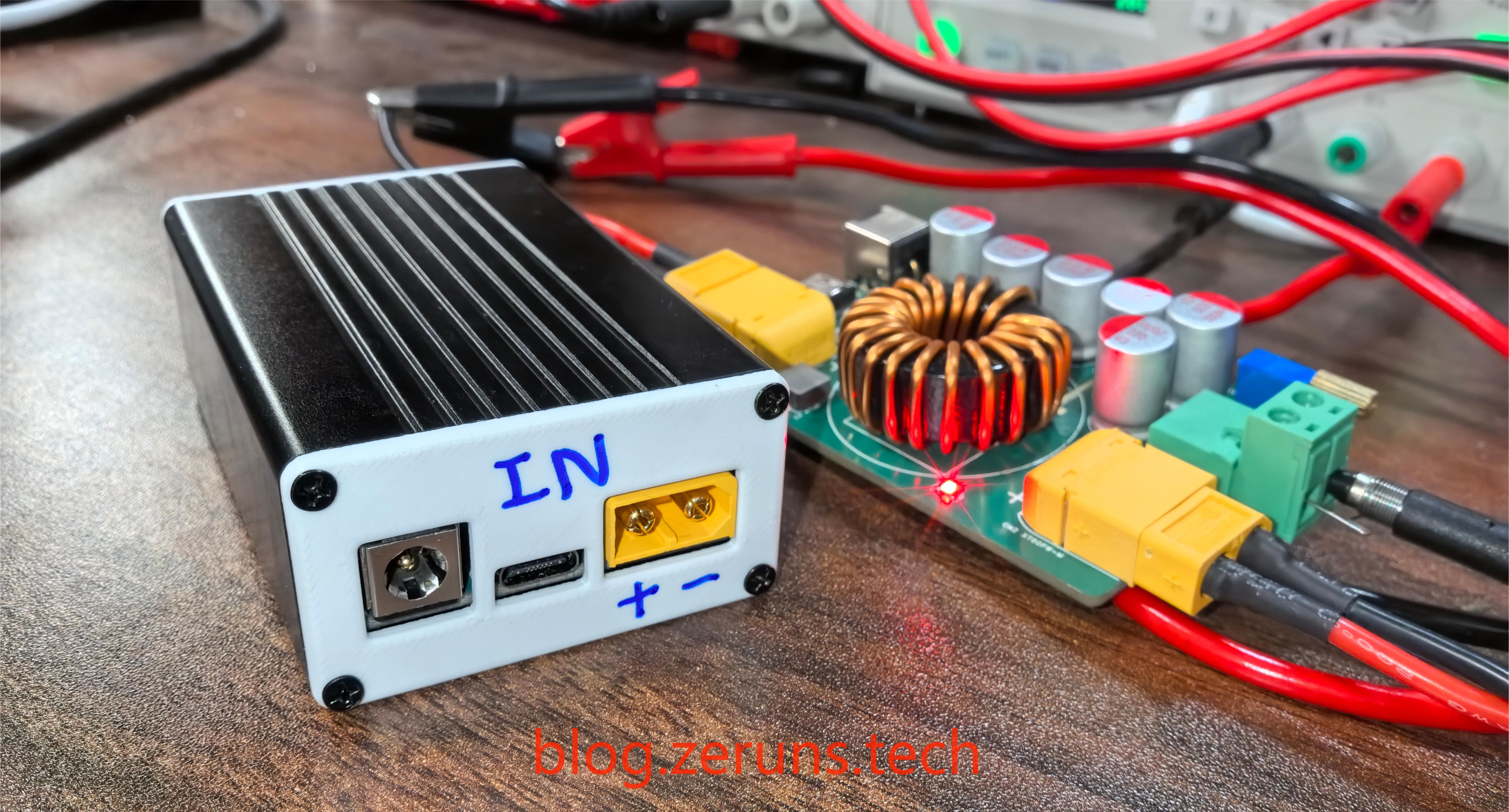
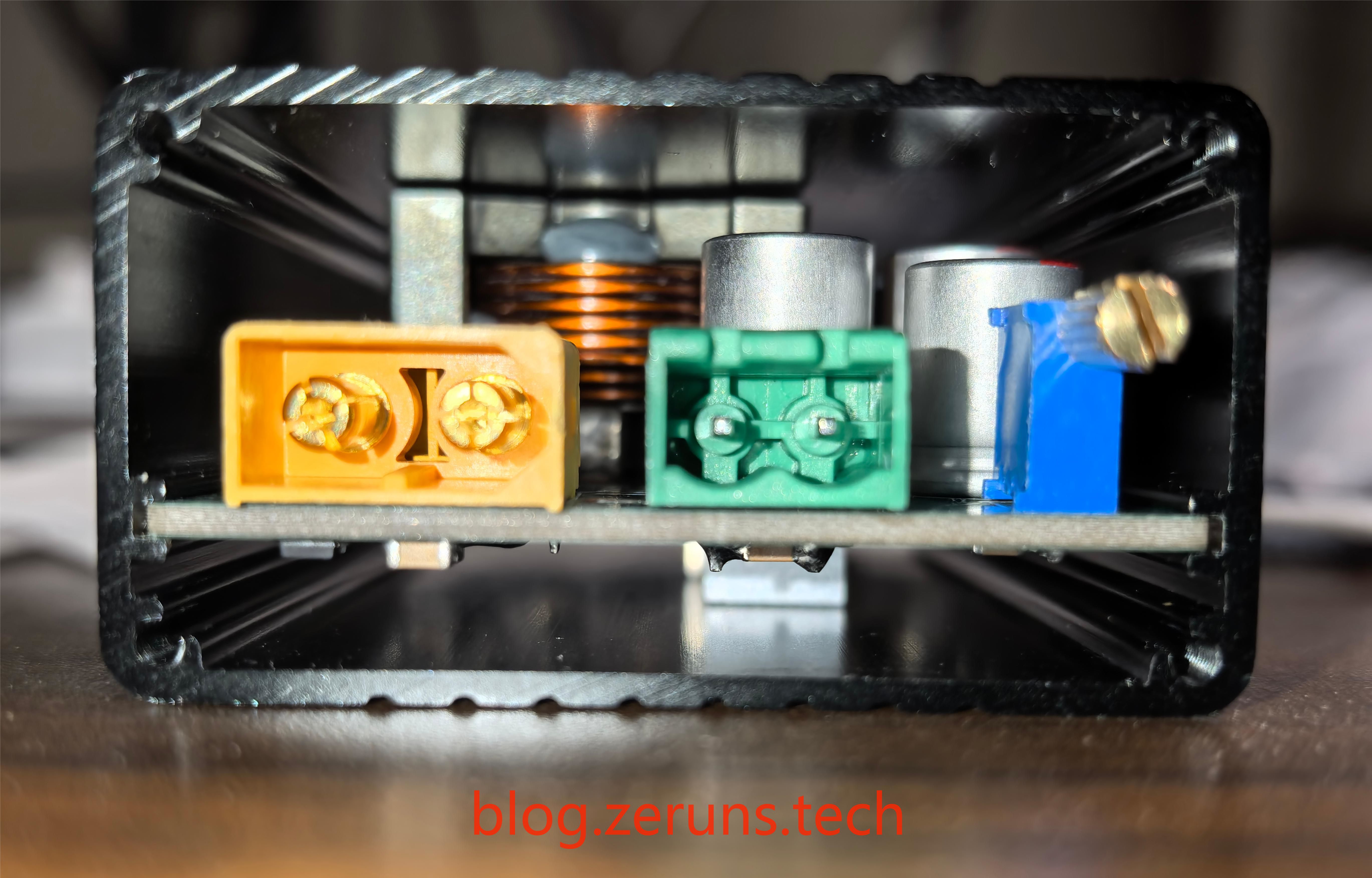
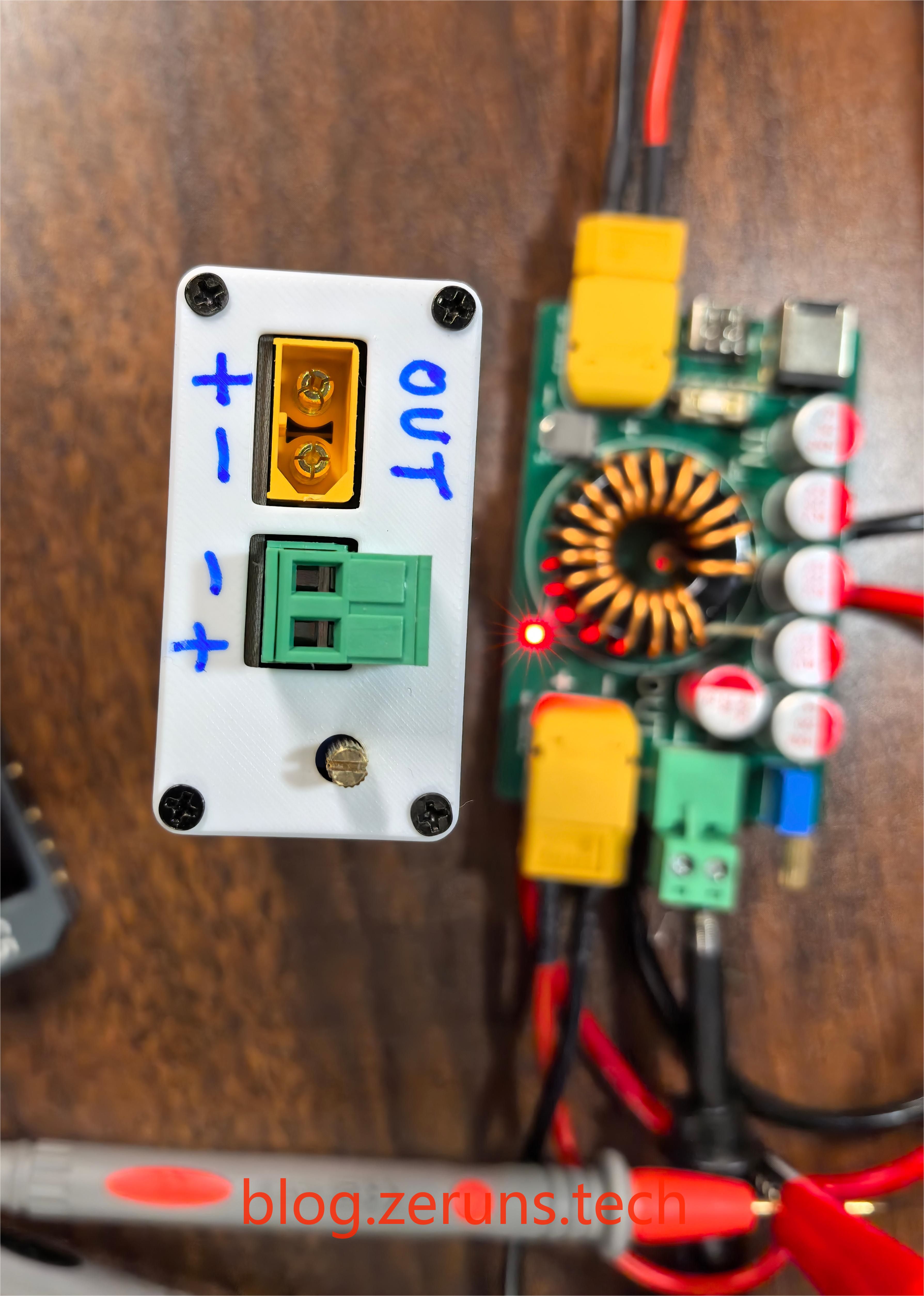
The enclosure is a purchased aluminum case from Taobao, while the front and rear covers were self-designed and 3D-printed. The 3D models of the enclosure and covers are also included in the resources.
Soldering Tips for the Chips
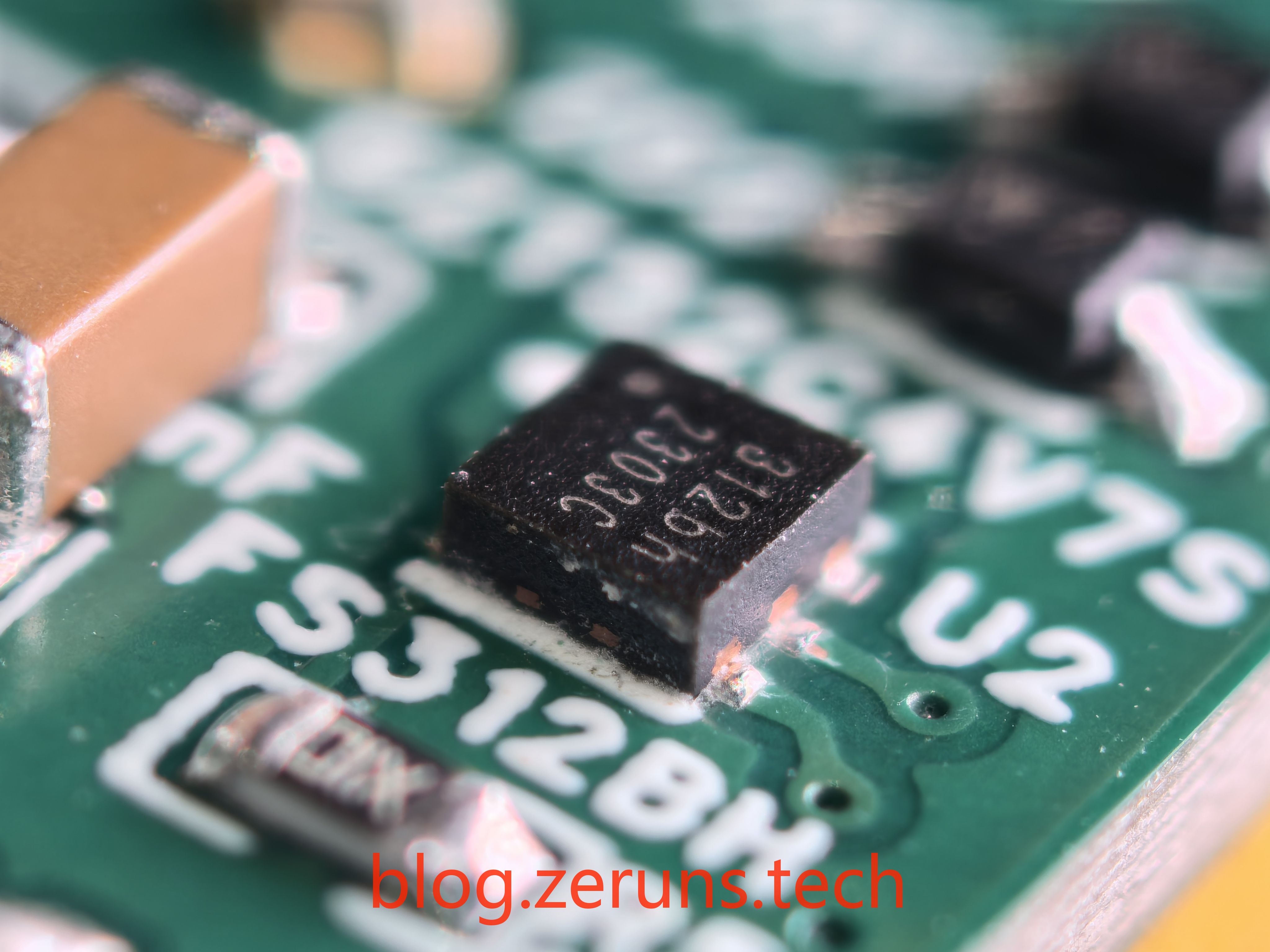
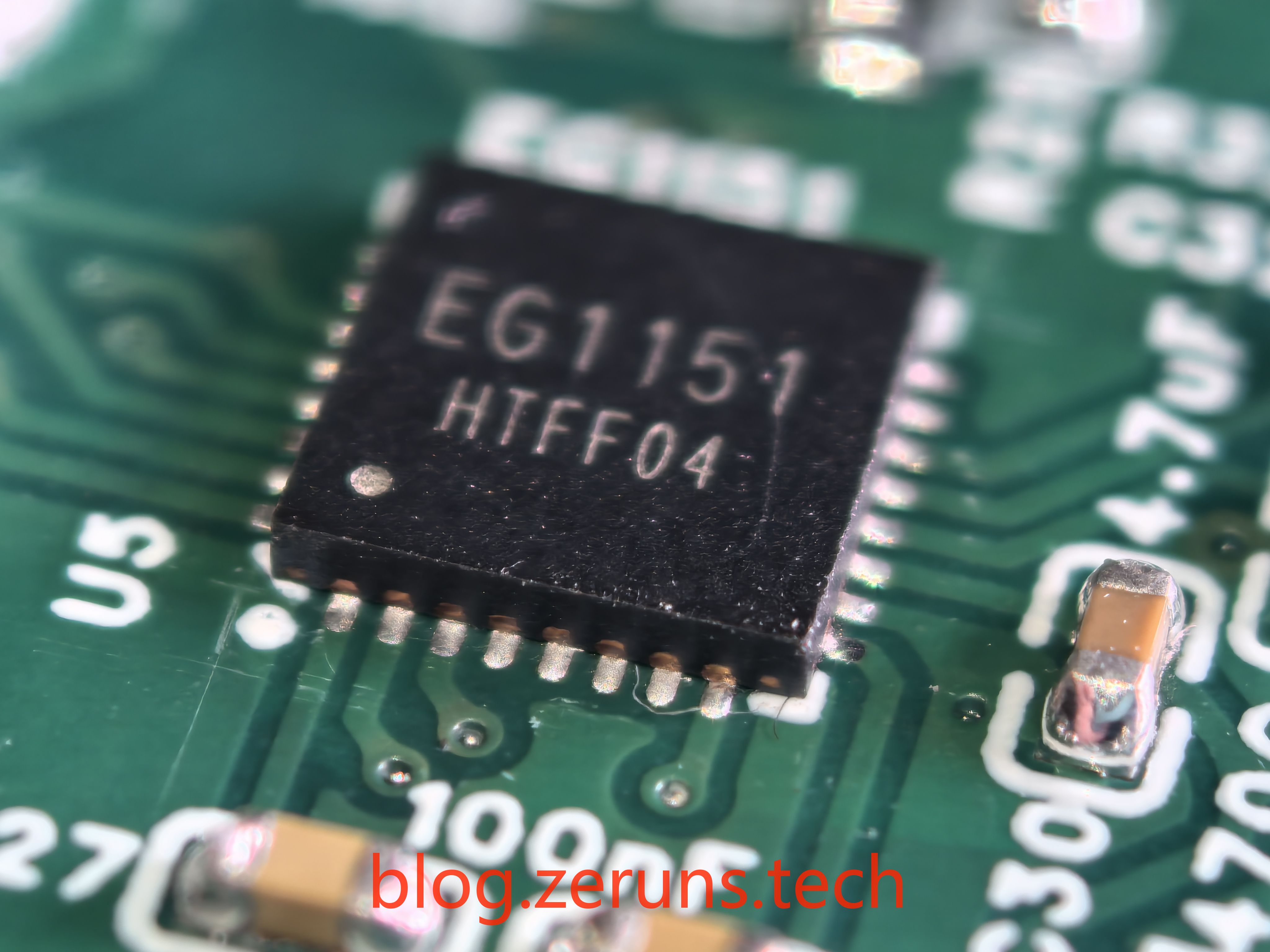
The EG1151 chip comes in a QFN32 package, and the FS312BH chip is in a DFN2X2-6L package. Both are very small and require some skill to solder properly.
When soldering these packages:
- For PCBs with an ENIG (Electroless Nickel Immersion Gold) finish, pre-tin the pads. For PCBs with a tin finish, pre-tin the chip pins.
- It is best to use low- or medium-temperature solder (high-temperature solder can make the process more difficult). For the center pad, apply just a small amount of solder. Excessive solder can lift the chip, preventing contact with surrounding pins. If excess solder is applied, clean the soldering iron and slowly remove the excess, or use desoldering braid.
- After tinning, apply solder flux to the pads, place the chip, and use a hot plate or hot air gun to heat the assembly. Once the solder melts, gently nudge the chip with tweezers to ensure it aligns itself. Let it cool, then check for solder bridges and fix them with a soldering iron if necessary.
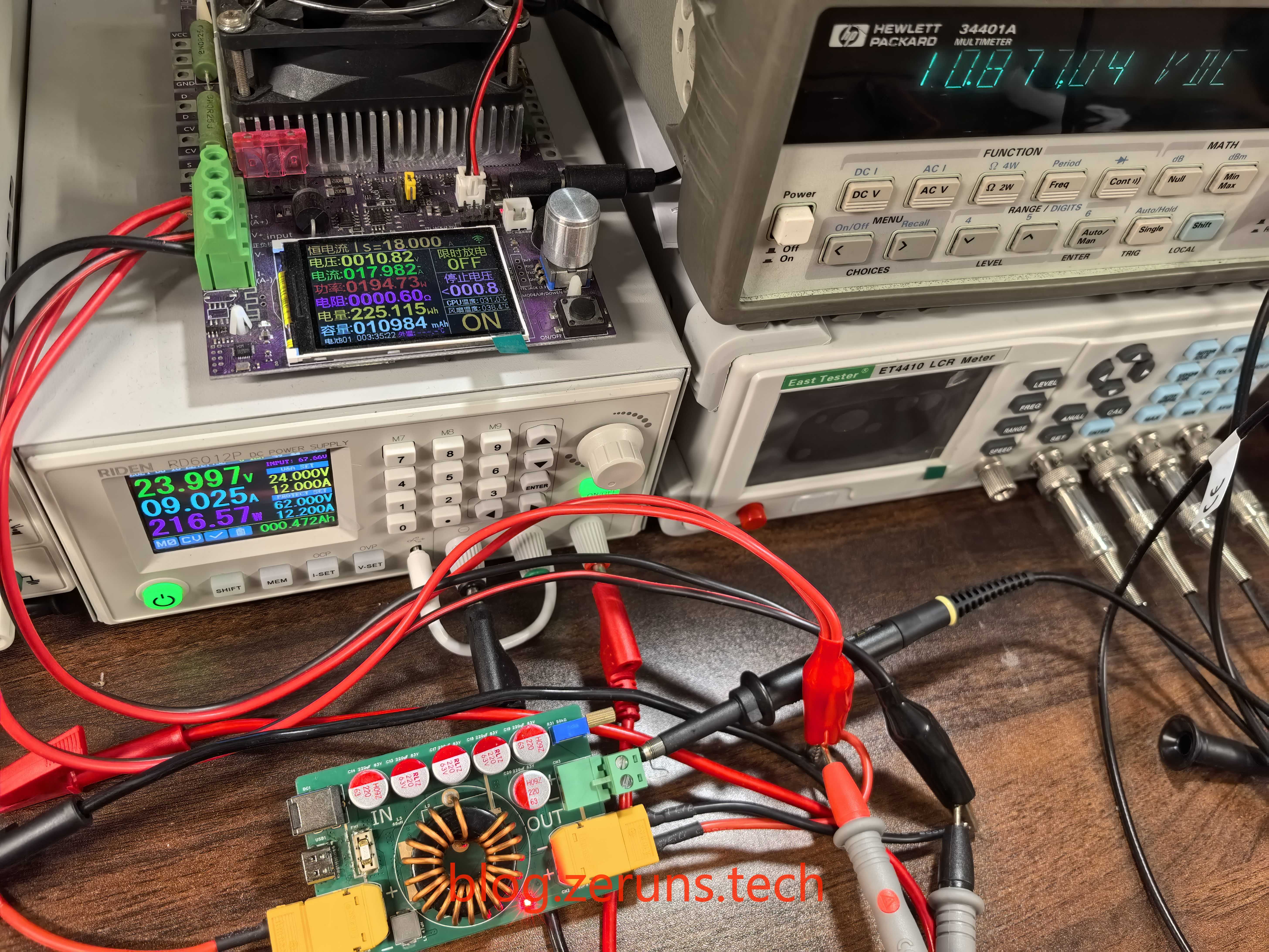
Testing
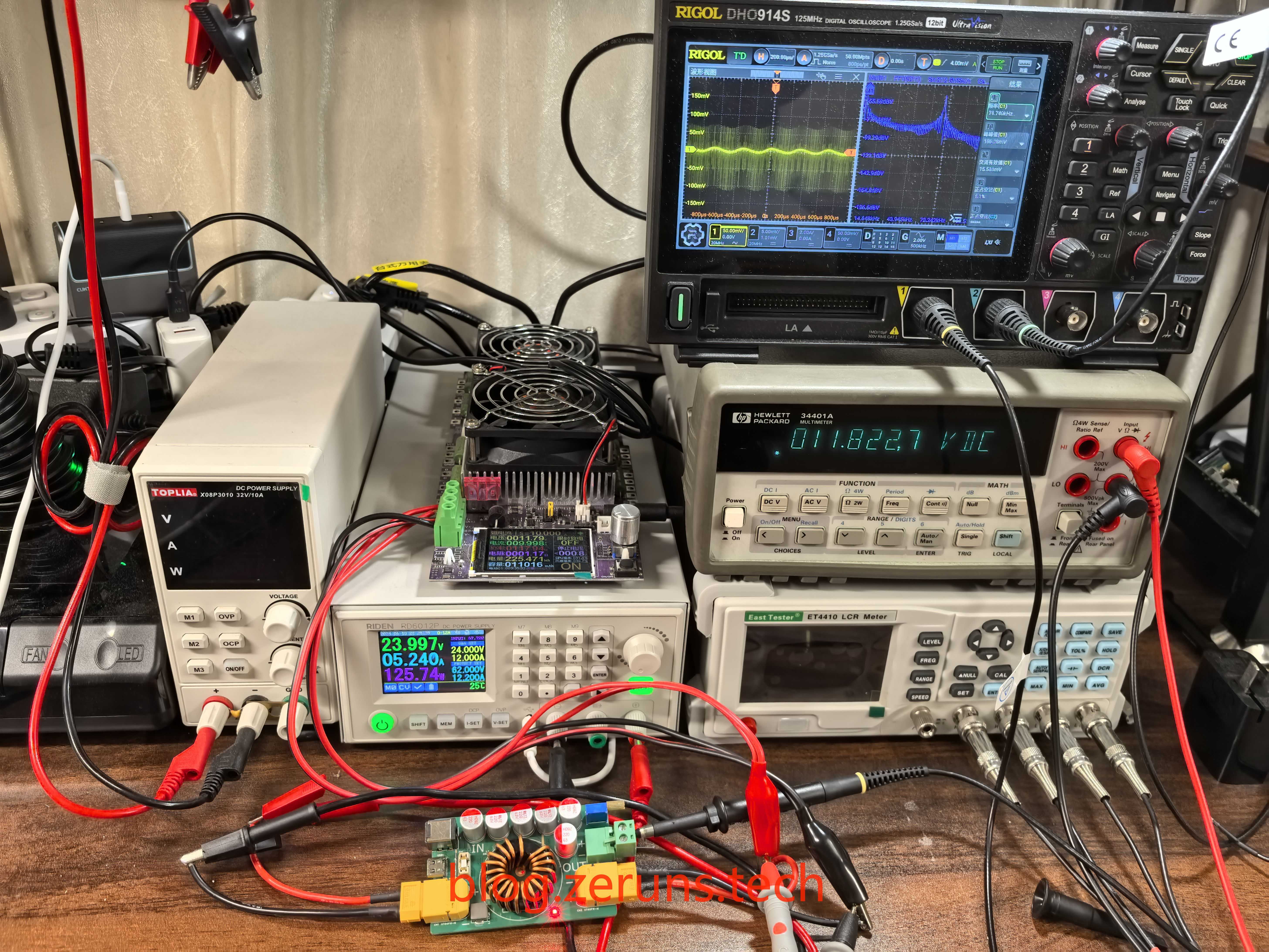
Using the XT60 connector, a 24V input was applied, with the XT60 output interface connected to a multimeter and an electronic load.
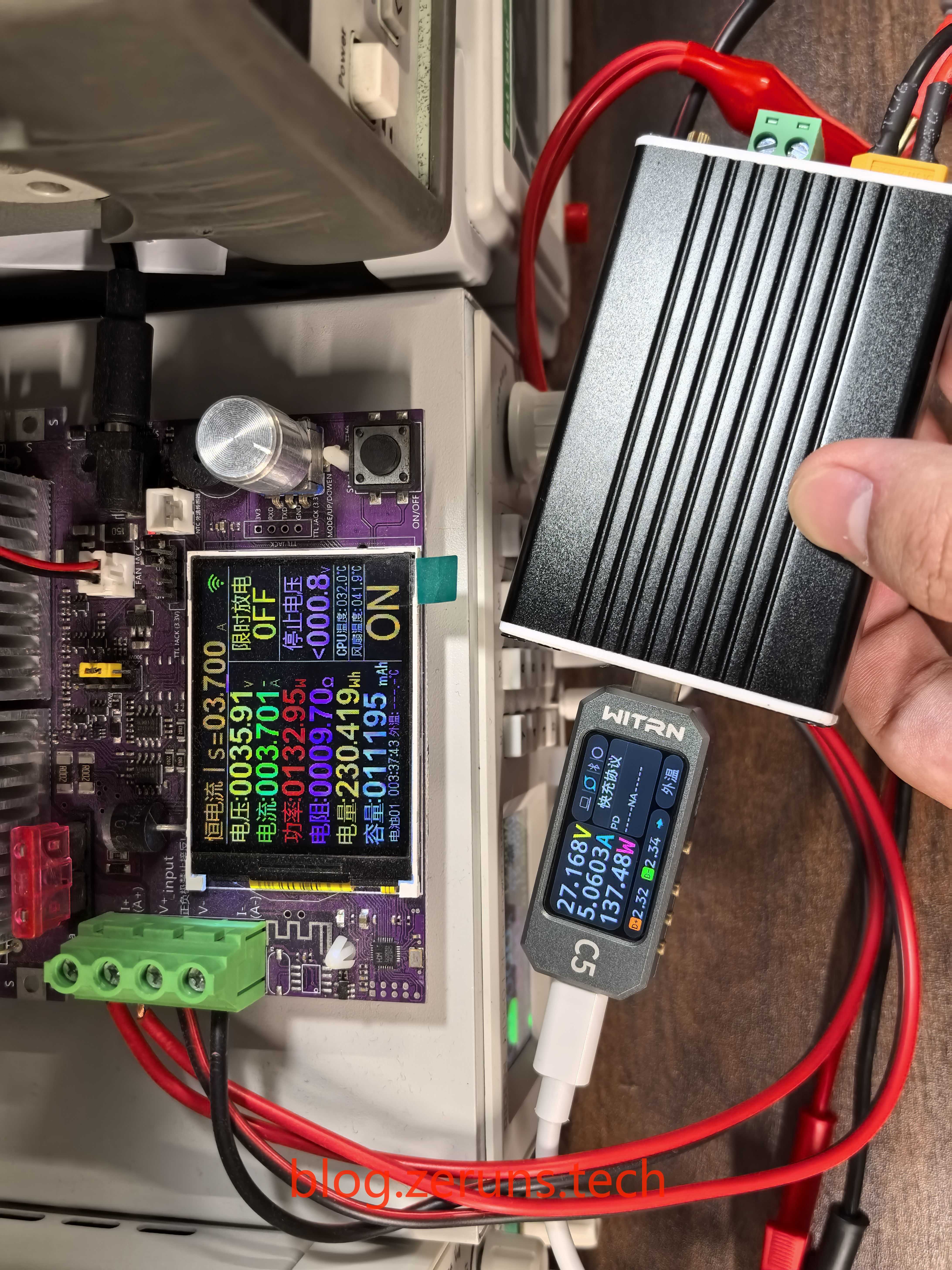
When a Type-C interface was used with a 140W PD3.1 charger from CoolGaN, the module successfully negotiated a 28V output.
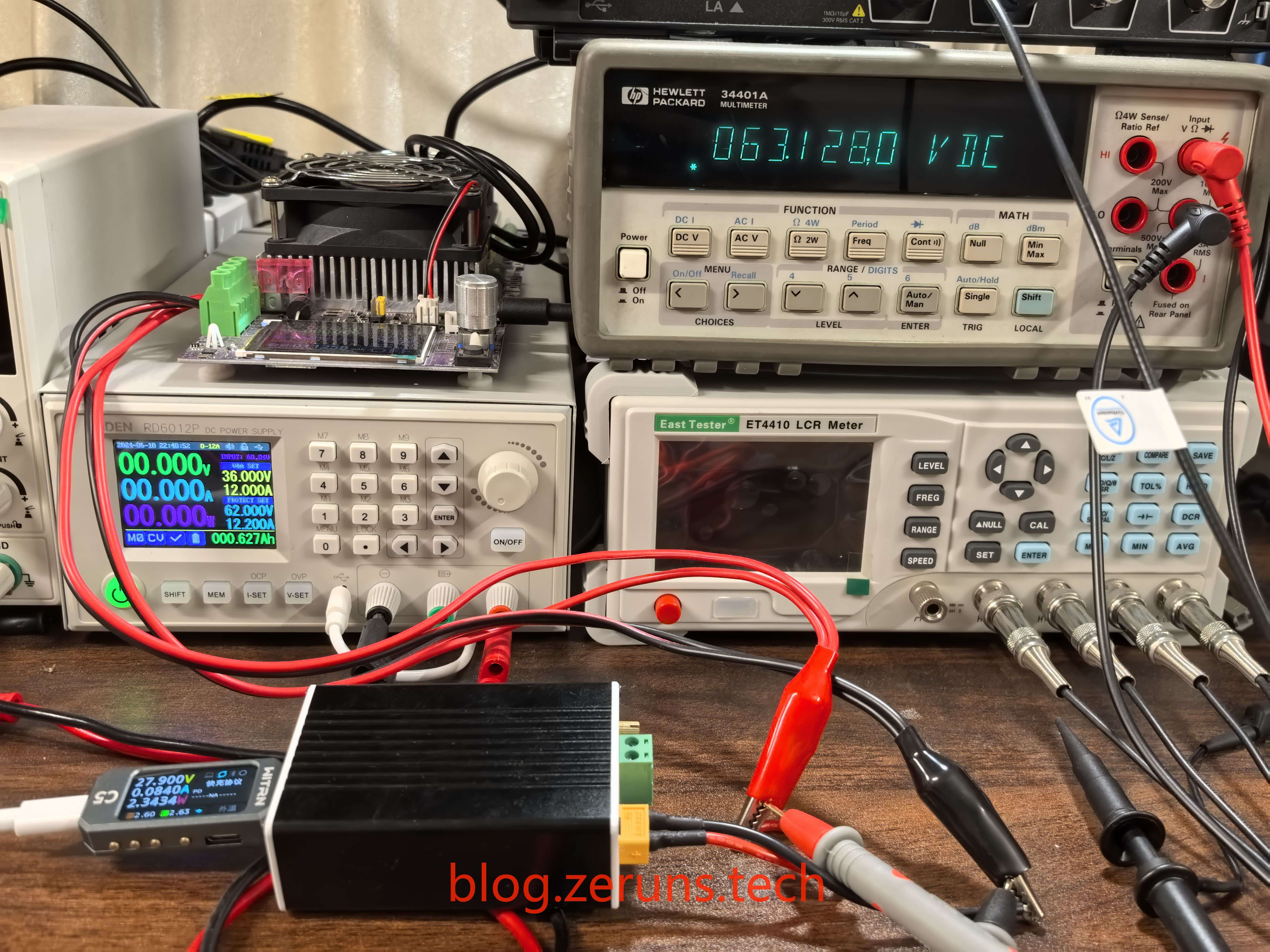
The maximum achievable output was 63V.
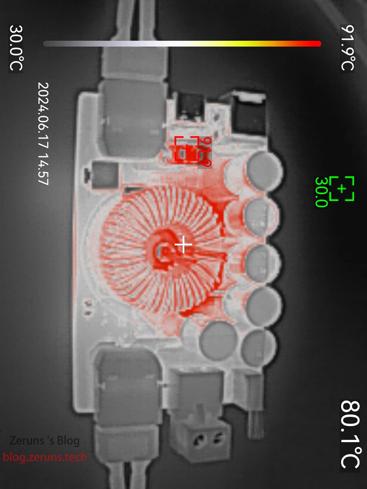
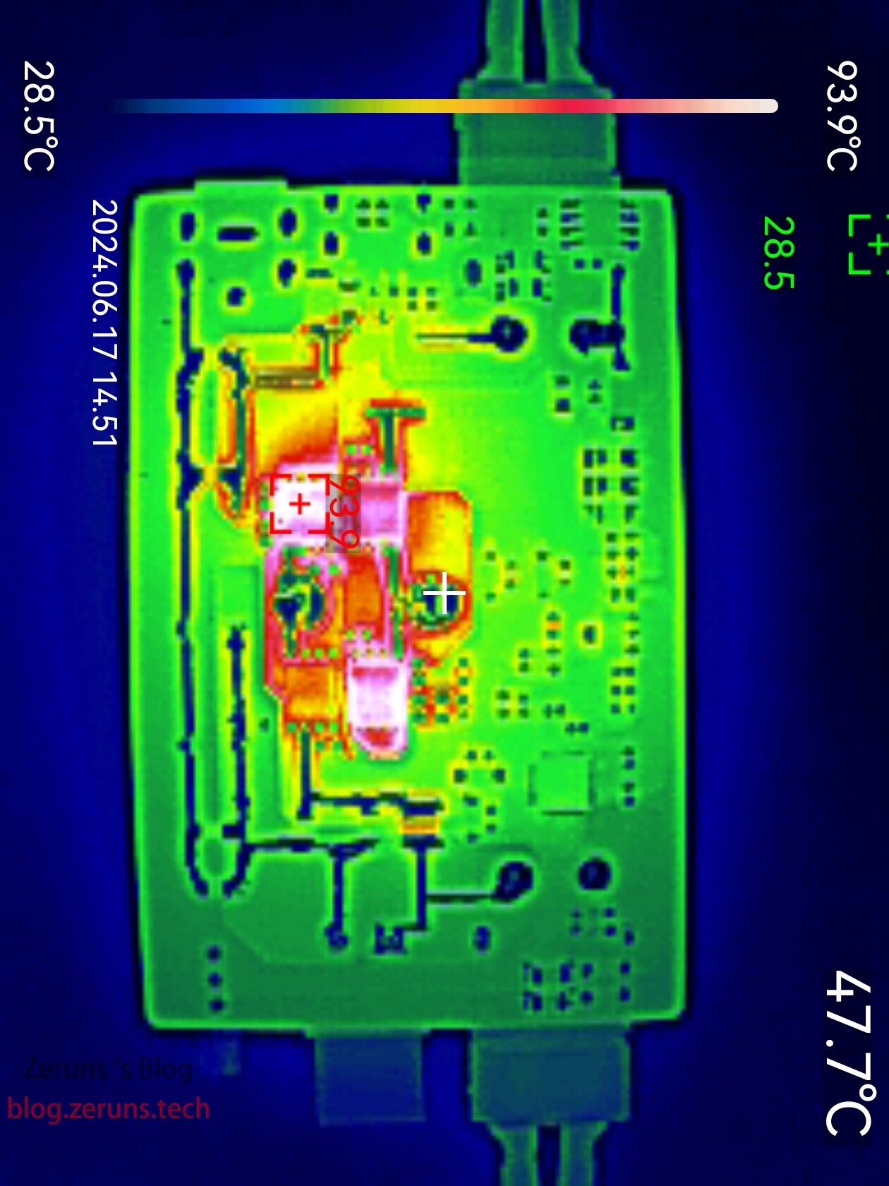
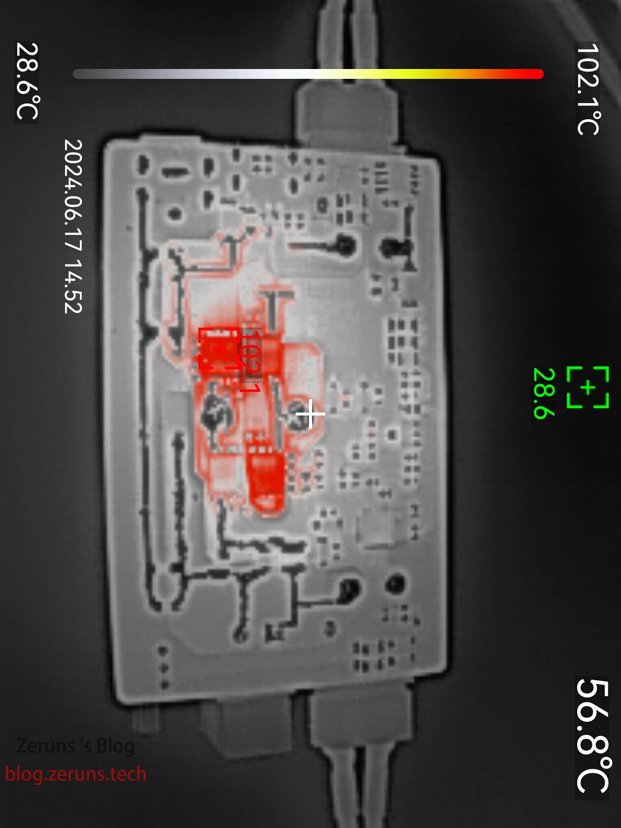
After a 10-minute run delivering 10A of current, a thermal imaging analysis showed that the MOSFET temperature was around 100°C. The contact resistance between the fuse and fuse holder appeared slightly high, contributing to localized heating.
Equipment Used for Testing:
- HP 34401A 6.5-digit multimeter: https://blog.zeruns.com/archives/772.html
- RuiDeng RD6012P programmable power supply: https://blog.zeruns.com/archives/740.html
- RIGOL DHO914S oscilloscope: https://blog.zeruns.com/archives/764.html
- Junwei electronic load: https://s.click.taobao.com/EdLEpkt
- UNI-T UTi261M thermal imaging camera review: https://blog.zeruns.com/archives/798.html
Conversion Efficiency Testing
The highest efficiency measured during testing was 96.869%.
The detailed test data are shown in the table below:
| Input Voltage (V) | Input Current (A) | Input Power (W) | Output Voltage (V) | Output Current (A) | Output Power (W) | Conversion Efficiency (%) |
|---|---|---|---|---|---|---|
| 36.000 | 6.932 | 249.552 | 48.194 | 4.996 | 240.777 | 96.484 |
| 60.000 | 6.264 | 375.840 | 35.669 | 9.995 | 356.512 | 94.857 |
| 48.000 | 9.434 | 452.832 | 28.841 | 14.993 | 432.413 | 95.491 |
| 60.000 | 5.941 | 356.460 | 18.430 | 17.988 | 331.519 | 93.003 |
| 60.000 | 4.270 | 256.200 | 12.129 | 18.990 | 230.330 | 89.902 |
| 12.001 | 10.913 | 130.967 | 24.003 | 5.002 | 120.063 | 91.674 |
| 25.000 | 9.915 | 247.875 | 23.749 | 10.008 | 237.680 | 95.887 |
| 12.004 | 9.889 | 118.708 | 36.068 | 3.002 | 108.276 | 91.213 |
| 12.004 | 2.291 | 27.501 | 5.070 | 5.000 | 25.350 | 92.178 |
| 12.004 | 9.130 | 109.597 | 10.116 | 10.013 | 101.292 | 92.422 |
| 48.000 | 7.812 | 374.976 | 36.188 | 10.005 | 362.061 | 96.556 |
| 48.000 | 8.658 | 415.584 | 50.315 | 8.001 | 402.570 | 96.869 |
Ripple Test
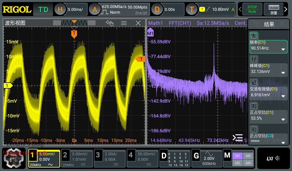
The ripple peak-to-peak voltage at 12V output with no load is approximately 32mV:
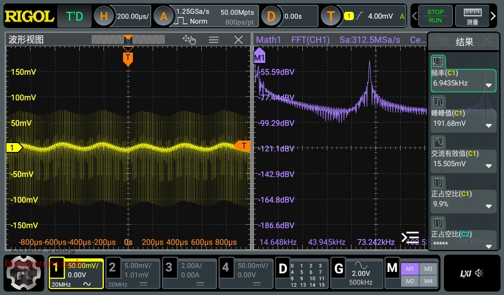
The ripple peak-to-peak voltage at 12V output with a 10A load is approximately 191mV:
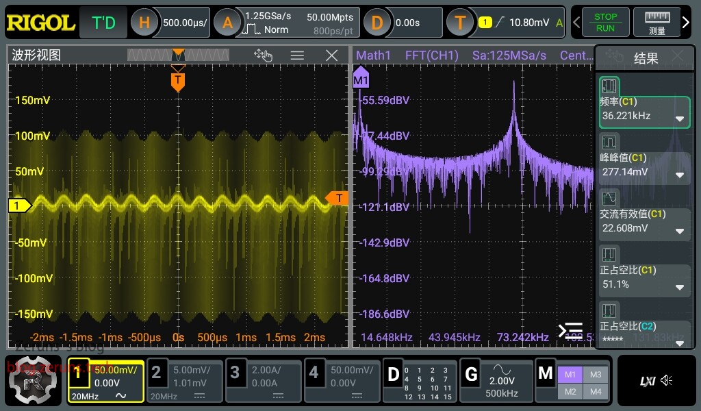
The ripple peak-to-peak voltage at 12V output with a 15A load is approximately 277mV:
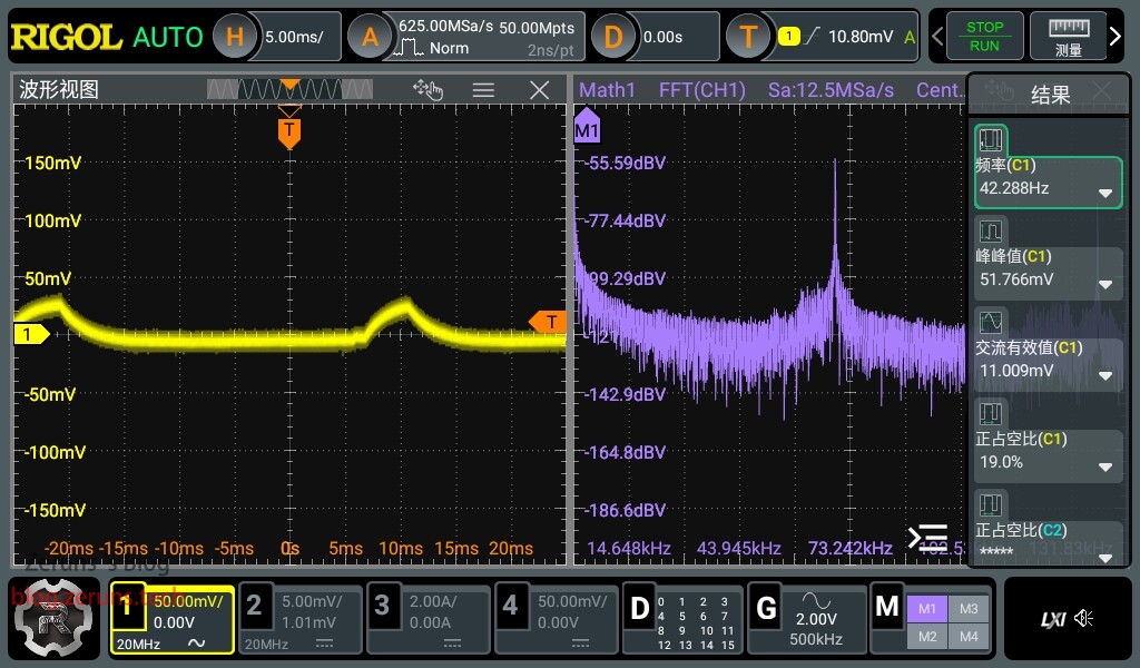
The ripple peak-to-peak voltage at 36V output with no load is approximately 51mV:
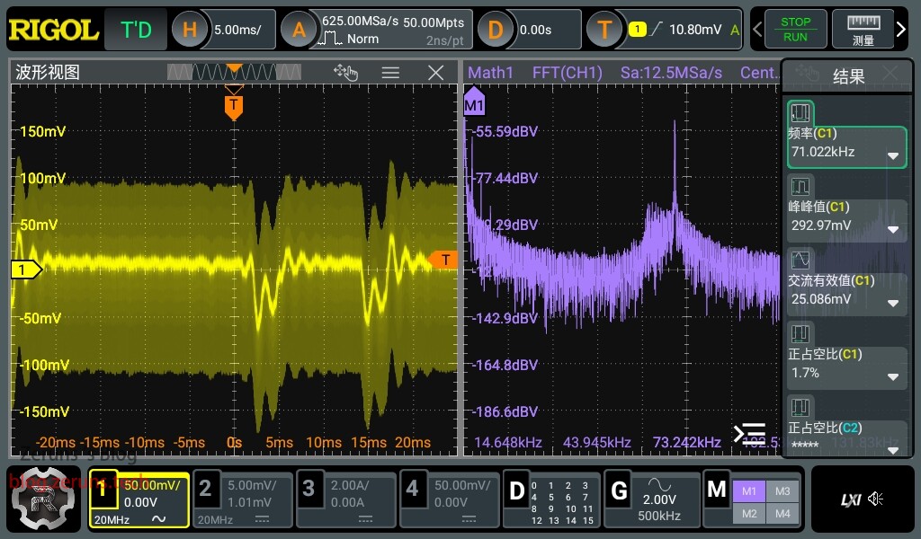
The ripple peak-to-peak voltage at 36V output with a 3A load is approximately 292mV:
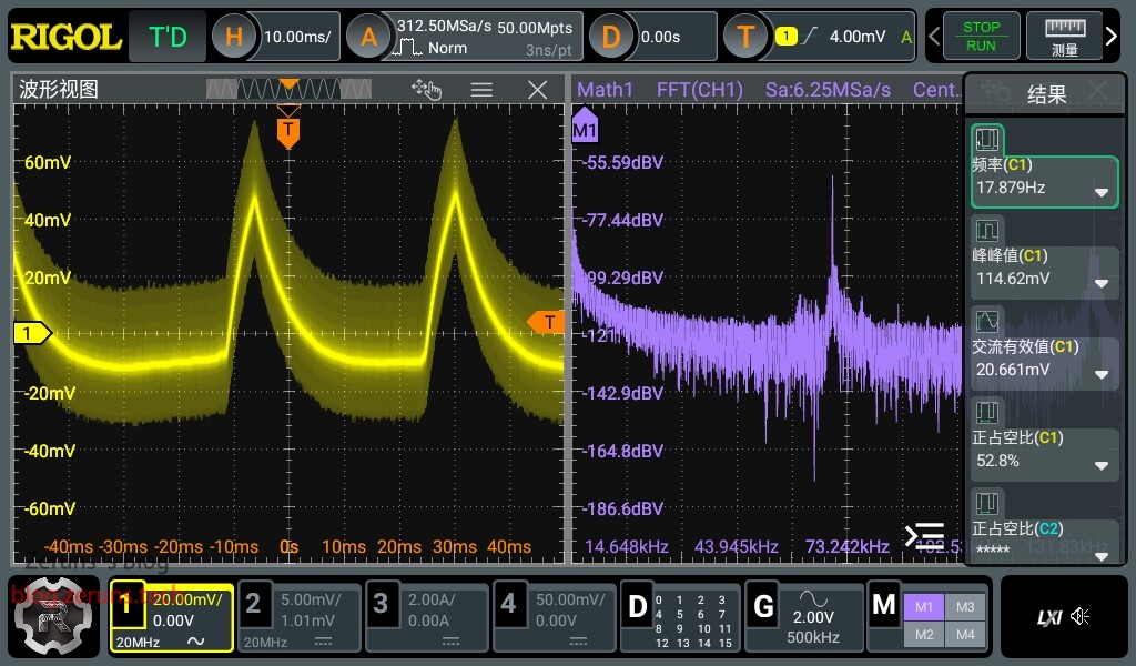
The ripple peak-to-peak voltage at 60V output with no load is approximately 114mV:
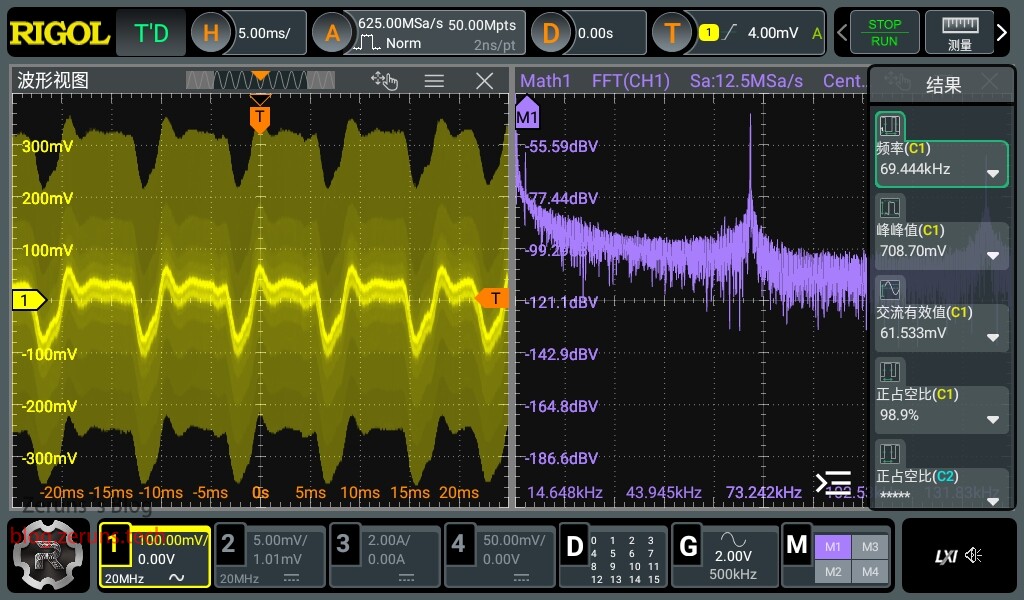
The ripple peak-to-peak voltage at 60V output with a 3A load is approximately 708mV:
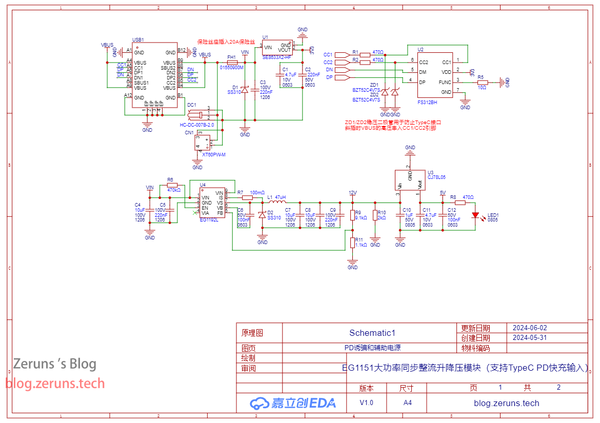
Schematic Diagram
Main Power Circuit:
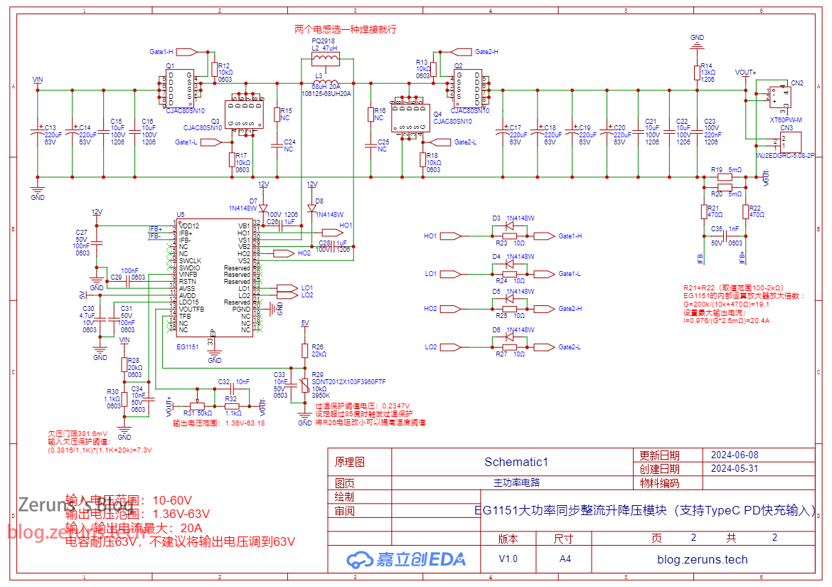
PD Negotiation and Auxiliary Power Circuit:
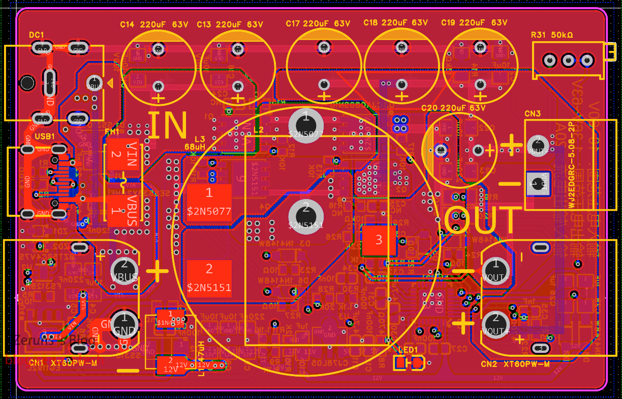
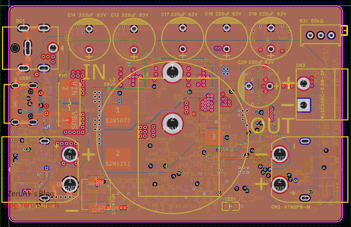
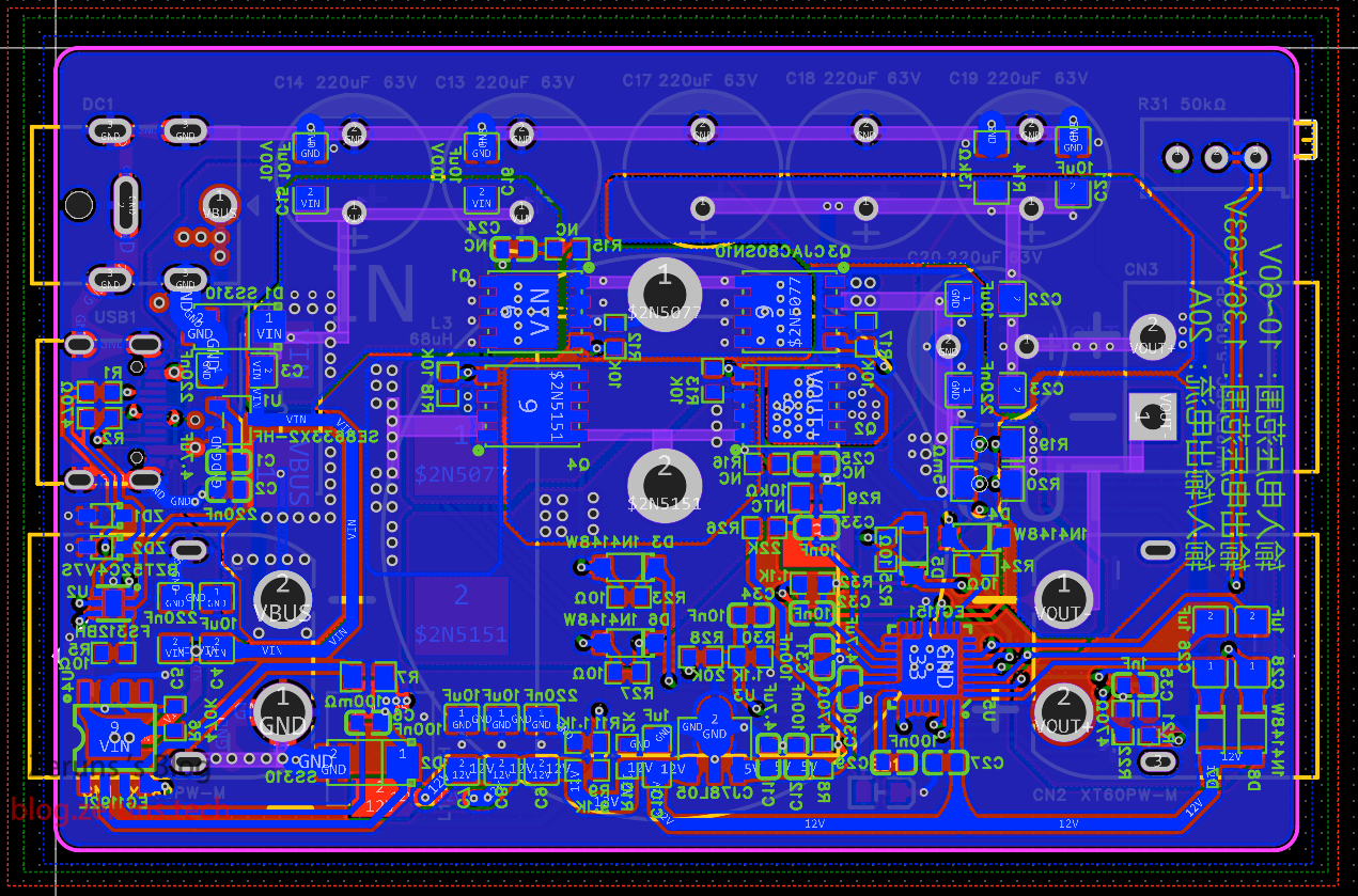
PCB
Top Layer:
Inner Layer 1:
Inner Layer 2:

Bottom Layer:
Component Purchase Links
Here are the purchase links for most components used in this project:
- 0603电阻电容样品本:https://s.click.taobao.com/SXT7pkt
- TypeC母座 16P:https://s.click.taobao.com/vjLRskt
- EG1151芯片:https://s.click.taobao.com/le3gAkt
- EG1192L芯片:https://s.click.taobao.com/pG2gAkt
- CJAC80SN10 MOS管:https://s.click.taobao.com/aPsWWlt
- XT60PW接口:https://s.click.taobao.com/6jZ7pkt
- 扁平线电感PQ2918 47μH:https://s.click.taobao.com/RDuLHkt
- 磁环电感 卧式 68μH 20A:https://s.click.taobao.com/8JHHcjt
- 铝合金外壳:https://s.click.taobao.com/fYK0zbt
It is recommended to purchase components from LCSC Mall: https://activity.szlcsc.com/invite/D03E5B9CEAAE70A4.html
By clicking "Order Now" in the BOM table link on the LCSC Open Source page, you can import the required components directly into your shopping cart.
Resource Download Links
The download links below include the following: LCSC EDA project files, schematic PDFs, datasheets for all used chips, and 3D model files for the enclosure.
- Baidu Cloud Download Link: https://pan.baidu.com/s/1gNl48K25p6Pr3gi9lsyMAg?pwd=tmsv
Extraction Code: tmsv - 123 Cloud Disk Download Link: https://www.123pan.com/s/2Y9Djv-r3tvH.html
Extraction Code: 0cGK
If you find this helpful, you can tip me via the 123 Cloud Disk link above. If you're reading a WeChat article (official account: zeruns-gzh), you can also click "Support Author" at the bottom of the article to send a tip. Thank you!
Other Recommended Open Source Projects
- Three-phase power consumption collector for monitoring household electricity usage (open source): https://blog.zeruns.com/archives/771.html
- STM32F407-based LVGL project template (MSP3526 screen), including FreeRTOS and bare-metal versions: https://blog.zeruns.com/archives/788.html
- Synchronous rectification Buck-Boost digital power supply based on STM32 (open source): https://blog.zeruns.com/archives/791.html
- LM25118 automatic Buck-Boost adjustable DC-DC power module: https://blog.zeruns.com/archives/727.html
- EG1164 high-power synchronous rectification boost module (open source) with 97% maximum efficiency: https://blog.zeruns.com/archives/730.html
- Air700E-based 4G environmental monitoring node (temperature, humidity, pressure, etc.), uploading data to Alibaba Cloud IoT via MQTT: https://blog.zeruns.com/archives/747.html
- CH32V307-based smart electronic load (open source), embedded competition project: https://blog.zeruns.com/archives/785.html
Recommended Reading
- Cost-effective and affordable VPS/cloud server recommendations: https://blog.zeruns.com/archives/383.html
- Minecraft server setup tutorials: https://blog.zeruns.com/tag/mc/
- Build your blog without coding! A detailed tutorial for personal blog setup: https://blog.zeruns.com/archives/783.html
- Intranet penetration server setup tutorial, NPS setup, and usage guide: https://blog.zeruns.com/archives/741.html
- RainCloud Ningbo 8272CL high-bandwidth anti-DDoS cloud server review (up to 500 Mbps bandwidth and 1TB cloud disk): https://blog.zeruns.com/archives/789.html
- TikTok Mall 120W charger for $2.60 - testing and teardown: https://blog.zeruns.com/archives/786.html


Comment Section